 Break Protected MCU PIC18F46K22 Flash Heximal Memory
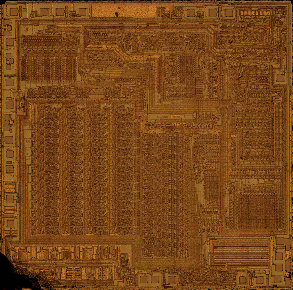
Break Protected MCU PIC18F46K22 Flash Heximal Memory and crack microcontroller pic18f46k22 protective fuse bit and readout locked firmware from MCU memory;
The data memory in PIC18 devices is implemented as static RAM. Each register in the data memory has a 12-bit address, allowing up to 4096 bytes of data memory. The memory space is divided into as many as 16 banks that contain 256 bytes each. Figures 5-5 through 5-7 show the data memory organization for the PIC18(L)F2X/4XK22 devices.
The data memory contains Special Function Registers (SFRs) and General Purpose Registers (GPRs). The SFRs are used for control and status of the controller and peripheral functions in order to replicate pic18f46k20 microprocessor flash program, while GPRs are used for data storage and scratchpad operations in the user’s application. Any read of an unimplemented location will read as ‘0’s.
The instruction set and architecture allow operations across all banks. The entire data memory may be accessed by Direct, Indirect or Indexed Addressing modes. Addressing modes are discussed later in this subsection.
To ensure that commonly used registers (SFRs and select GPRs) can be accessed in a single cycle, PIC18 devices implement an Access Bank. This is a 256-byte memory space that provides fast access to SFRs and the lower portion of GPR Bank 0 without using the Bank Select Register (BSR). Section 5.3.2 “Access Bank” provides a detailed description of the Access RAM.