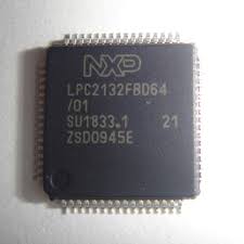
 Break IC LPC2132FBD64 Firmware
In the field of embedded electronics, the LPC2132FBD64 microcontroller—based on the ARM7TDMI-S core—is widely used in applications ranging from industrial control to medical devices and consumer electronics. With its integrated 512KB Flash memory, rich peripheral set, and advanced features, it has become a reliable choice for secure embedded system design. However, its protected and encrypted firmware often poses a significant obstacle when users need to regain access to a device’s functionality or replicate legacy systems. That’s where we come in.
At CIRCUIT ENGINEERING CO.,LTD, we specialize in providing professional services to break IC LPC2132FBD64 firmware, allowing end users and engineers to unlock, copy, and restore the internal code of secured and locked microcontrollers. Whether it’s for product repair, legacy system recovery, or R&D, our solutions are designed to disable fuse bits, bypass read protection, and extract data securely and confidentially.
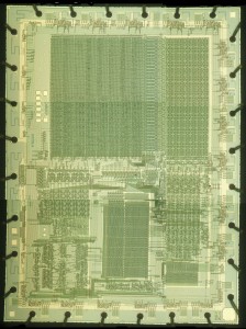
Break IC LPC2132FBD64 program memory and readout firmware from Microcontroller LPC2132FBD64, focus ion beam technique will be applied to reset the status of MCU LPC2132FBD64 from locked to unlocked one;
The LPC2132 microcontrollers are based on a 32/16 bit ARM7TDMI-S CPU with real-time emulation and embedded trace support, that combines the microcontroller with 32 kB, 64 kB, 128 kB, 256 kB and 512 kB of embedded high speed Flash memory.
Manufacturers often implement security features in microcontrollers like the LPC2132FBD64 to lock the firmware and prevent unauthorized access. While this protects intellectual property, it can become problematic for legitimate users when the original developer is unavailable, the firmware is lost, or a system needs modification. The chip’s security bits and fuse protections are intentionally designed to prevent reading of the flash, EEPROM, or memory archive, even with direct access to the device.
Using proprietary techniques and custom hardware interfaces, our team can carefully crack, decode, and read out the binary or heximal firmware of the LPC2132FBD64 without damaging the hardware. We also offer advanced decryption and disassembly services to convert the extracted data into readable source code or program files, enabling full analysis, reuse, or migration to other platforms.
The LPC2132FBD64 is valued for its compact 64-pin LQFP package and high-speed 60MHz CPU operation. It features two 10-bit ADCs, multiple UARTs, SPI/I2C interfaces, PWM channels, and USB 1.1 full-speed support—making it a powerful and versatile microcontroller in embedded system design. These rich peripherals are often deeply tied into the firmware, meaning that gaining access to the code is crucial for re-implementation, debugging, or custom development.
A 128-bit wide memory interface and a unique accelerator architecture enable 32-bit code execution at maximum clock rate. For critical code size applications, the alternative 16-bit Thumb mode reduces code by more than 30 % with minimal performance penalty after Copying IC PIC16F84A binary.
Our Complete Service Offering
- Firmware extraction from locked LPC2132FBD64 ICs
- Fuse bit disablement and read protection bypass
- Binary and heximal data recovery
- Conversion to C-style source code or annotated assembly
- Cloning and duplication for system replication
- Secure handling and confidential data management
Our services are trusted by electronics repair centers, product manufacturers, forensic investigators, and reverse engineering specialists. We treat each project with strict confidentiality and provide documentation of the process upon request.
Due to their tiny size and low power consumption, these microcontrollers are ideal for applications where miniaturization is a key requirement, such as access control and point-of-sale. With a wide range of serial communications interfaces and on-chip SRAM options of 8/16/32 kB, they are very well suited for communication gateways and protocol converters, soft modems, voice recognition and low end imaging, providing both large buffer size and high processing power. Various 32-bit timers, single or dual 10-bit 8 channel ADC(s), 10-bit DAC, PWM channels and 47 GPIO lines with up to nine edge or level sensitive external interrupt pins make these microcontrollers particularly suitable for industrial control and medical systems after attacking C8051F530 firmware.
16/32-bit ARM7TDMI-S microcontroller in a tiny LQFP64 package.
8/16/32 kB of on-chip static RAM and 32/64/128/256/512 kB of on-chip Flash program memory. 128 bit wide interface/accelerator enables high speed 60 MHz operation. In-System/In-Application Programming (ISP/IAP) via on-chip boot-loader software.
Single Flash sector or full chip erase in 400 ms and programming of 256 bytes in 1 ms. EmbeddedICE RT and Embedded Trace interfaces offer real-time debugging with the on-chip RealMonitor software and high speed tracing of instruction execution.
One (LPC2132) or two (LPC2134/36/38) 8 channel 10-bit A/D converters provides a total of up to 16 analog inputs, with conversion times as low as 2.44 µs per channel. Single 10-bit D/A converter provides variable analog output (LPC2132). Two 32-bit timers/external event counters (with four capture and four compare channels each), PWM unit (six outputs) and watchdog after attack microcontroller PIC16C63A heximal.
Low power Real-time clock with independent power and dedicated 32 kHz clock input.
Multiple serial interfaces including two UARTs (16C550), two Fast I2C-bus (400 kbit/s),
SPI and SSP with buffering and variable data length capabilities.
Vectored interrupt controller with configurable priorities and vector addresses.
Up to 47 5 V tolerant general purpose I/O pins in tiny LQFP64 package.
Up to nine edge or level sensitive external interrupt pins available.
60 MHz maximum CPU clock available from programmable on-chip PLL with settling time of 100 µs.
On-chip integrated oscillator operates with external crystal in range of 1 MHz to
30 MHz and with external oscillator up to 50 MHz.
Power saving modes include Idle and Power-down
Individual enable/disable of peripheral functions as well as peripheral clock scaling down for additional power optimization.
Processor wake-up from Power-down mode via external interrupt or BOD.
Single power supply chip with POR and BOD circuits:
CPU operating voltage range of 3.0 V to 3.6 V (3.3 V ± 10 %) with 5 V tolerant I/O pads.