Archive for November, 2012
 Dump Microcontroller ATMEGA1284V Source Code
We can dump microcontroller ATMEGA1284V source code, please view the microcontroller ATMEGA1284V features for your reference:
This bit is set (one) when an ADC conversion completes and the data registers are updated. The ADC Conversion Complete Interrupt is executed if the ADIE bit and the I-bit in SREG are set (one).
ADIF is cleared by hardware when executing the corresponding interrupt handling vector. Alternatively, ADIF is cleared by writing a logical “1” to the flag.
Beware that if doing a read-modify-write on ADCSR, a pending interrupt can be disabled. This also applies if the SBI and CBI instructions are used before Dump Microcontroller ATMEGA1284V Source Code.
· Bit 3 – ADIE: ADC Interrupt Enable
When this bit is set (one) and the I-bit in SREG is set (one), the ADC Conversion Complete Interrupt is activated.
· Bits 2..0 – ADPS2..ADPS0: ADC Prescaler Select Bits
These bits determine the division factor between the CK frequency and the input clock to the ADC. When an ADC conversion is complete, the result is found in these two registers.
When ADCL is read, the ADC Data Register is not updated until ADCH is read. If the result is left adjusted and no more than 8-bit precision is required, it is sufficient to read ADCH.
Otherwise, ADCL must be read first, then ADCH. The ADLAR bit in ADMUX affects the way the result is read from the registers. If ADLAR is set, the result is left-adjusted if Dump Microcontroller ATMEGA1284V Source Code.
If ADLAR is cleared (default), the result is right-adjusted.
· ADC9..0: ADC Conversion Result
These bits represent the result from the conversion. For the differential channel, this is the value after gain adjustment, as indicated in Table 20 on page 47. For single-ended conversion, or if ADLAR or SIGN is zero, $000 represents ground and $3FF represents the selected reference voltage minus one LSB.
Since change of analog channel always is delayed until a conversion is finished, the Free Running mode can be used to scan multiple channels without interrupting the converter.
Typically, the ADC Conversion Complete Interrupt will be used to perform the channel shift. However, the user should take the following fact into consideration:
The interrupt triggers once the result is ready to be read. In Free Running mode, the next conversion will start immediately when the interrupt triggers. If ADMUX is changed after the interrupt triggers, the next conversion has already started, and the old setting is used if Dump Microcontroller ATMEGA1284V Source Code.
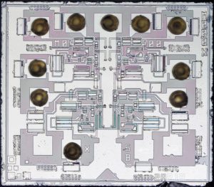
Brute Force IC Break Example
Brute Force IC Break is a process through which the inner circuitry pattern of MCU will be changed include decapsulation, focus ion beam and laser cut ways;
Brute force IC break’s one good example could be the password protection scheme used in microcontrollers, such as the Texas Instruments MSP430 family. The password itself is 32 bytes (256 bits) long which is more than enough to withstand direct brute force MCU breaking methods.

Brute Force IC Break is a process through which the inner circuitry pattern of MCU will be changed include decapsulation, focus ion beam and laser cut ways
But the password is allocated at the same memory addresses as the CPU interrupt vectors. That, firstly, reduces the area of search as the vectors always point to even addresses within memory. Secondly, when the software gets updated, only a small part of the password is changed because most of the interrupt subroutines pointed to by the vectors are very likely to stay at the same addresses.
As a result, if the IC code extractor knows one of the previous passwords he could easily do a systematic search and find the correct password in a reasonable time.
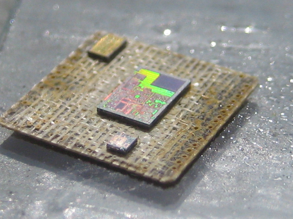
Brute Force Chip Attack
Brute Force Chip Attack include invasive and semi-invasive microcontroller cracking, hardware attacking will be able to get access to embedded memory such as flash and eeprom memory, then readout firmware from Microprocessor memory;
Brute Force Chip Attack include invasive and semi-invasive microcontroller cracking, hardware attacking will be able to get access to embedded memory such as flash and eeprom memory, then readout firmware from Microprocessor memory
MCU Attack has different meanings for cryptography and semiconductor hardware. In cryptography, a brute force chip attack would be defined as the methodical application of a large set of trials for a key to the system. This is usually done with a computer or an array of FPGAs delivering patterns at high speed and looking for success.
Decrypt IC ATmega640P Secured Code
We can decrypt IC ATMEGA640P secured code, please view the IC ATMEGA640P features for your reference:
Digital circuitry inside and outside the ATmega640P generates EMI, which might affect the accuracy of analog measurements. If conversion accuracy is critical, the noise level can be reduced by applying the following techniques:
1. The analog part of the ATmega640P and all analog components in the application should have a separate analog ground plane on the PCB. This ground plane is connected to the digital ground plane via a single point on the PCB.
2. Keep analog signal paths as short as possible. Make sure analog tracks run over the analog ground plane, and keep them well away from high-speed switching digital tracks before Decrypt IC ATmega640P Secured Code.
3. Use the ADC noise canceler function to reduce induced noise from the CPU.
4. If some Port B pins are used as digital outputs, it is essential that these do not switch while a conversion is in progress.
All AVR ports have true read-modify-write functionality when used as general digital I/O ports. This means that the direction of one port pin can be changed without unintentionally changing the direction of any other pin with the SBI and CBI instructions.
The same applies for changing drive value (if configured as output) or enabling/disabling of pull-up resistors (if configured as input). Port B is a 6-bit bi-directional I/O port when Decrypt IC ATmega640P Secured Code.
Three data memory address locations are allocated for Port B, one each for the Data Register – PORTB, $18, Data Direction Register – DDRB, $17, and the Port B Input Pins – PINB, $16. The Port B Input Pins address is read-only, while the Data Register and the Data Direction Register are read/write.
Ports PB5..0 have special functions as described in the section “Pin Descriptions” on page 4. If PB5 is not configured as external reset, it is input with no pull-up or as an open-drain output.
All I/O pins have individually selectable pull-ups, which can be over- ridden with pull-up disable. The Port B output buffers on PB0 to PB4 can sink 20 mA and thus drive LED displays directly before decrypt IC secured code.
PB5 can sink 12 mA. When pins PB0 to PB4 are used as inputs and are externally pulled low, they will source current (IIL) if the internal pull-ups are activated after BREAK IC.
How to Prevent MCU Timing Attack
To prevent MCU timing attacks, the designer should carefully calculate the number of CPU cycles that take place when the password is compared and make sure they are the same for correct and incorrect passwords. For example, in the Motorola 68HC08 microcontrollers family the internal ROM bootloader allows access to the Flash memory only if the correct eight-byte password was entered first.
To achieve that, extra NOP commands were added to the program making the processing time equal for both correct and incorrect bytes of the password. That gives good protection against MCU timing attacks. Some microcontrollers have an internal RC generator mode of operation in which the CPU running frequency depends upon the power supply voltage and the die temperature which will greatly increase the difficulty of MCU cracking.
This makes timing analysis more difficult as the MCU attacker has to stabilize the device temperature and reduce any fluctuations and noise on the power supply line. Some smartcards have an internally randomised clock signal to make measurements of the time delays useless for the attack.
Reverse Engineering Chip ATmega640PV Locked Flash
We can reverse engineering chip ATMEGA640PV locked flash, please view the chip ATMEGA640PV features for your reference:
In ATmega640PV four Port B pins – PB2, PB3, PB4, and PB5 – have alternative functions as inputs for the ADC. If some Port B pins are configured as outputs, it is essential that these do not switch when a conversion is in progress.
This might corrupt the result of the conversion. During Power-down mode and ADC Noise Reduction mode, the Schmitt triggers of the digital inputs are disconnected on these pins if reverse engineering chip locked flash.
This allows an analog input voltage close to VCC/2 to be present during Power-down without causing excessive power consumption. The Port B pins with alternate functions are shown in Table 1 on page 4.
When the pins PB4..0 are used for the alternate function, the DDRB and PORTB registers have to be set according to the alternate function description. When PB5 is used as external reset pin, the values in the corresponding DDRB and PORTB bit are ignored after Reverse Engineering Chip ATmega640PV Locked Flash.
The Port B Input Pins address (PINB) is not a register, and this address enables access to the physical value on each Port B pin. When reading PORTB, the PORTB Data Latch is read, and when reading PINB, the logical values present on the pins are read.
The lower five pins in Port B are equal when used as digital I/O pins. PBn, general I/O pin: The DDBn bit in the DDRB register selects the direction of this pin if Reverse Engineering Chip ATmega640PV Locked Flash.
If DDBn is set (one), PBn is configured as an output pin. If DDBn is cleared (zero), PBn is configured as an input pin. If PORTBn is set (one) when the pin is configured as an input pin, the MOS pull-up resistor is activated.
To switch the pull-up resistor off, the PORTBn has to be cleared (zero) or the pin has to be configured as an output pin. Pull-ups for all ports can be disabled also by setting PUD-bit in the MCUCR register.
Timing Attack Application
Timing attacks can be applied to microcontrollers whose security protection is based on passwords, or to access control systems that use cards or keys with fixed serial numbers, for example, Dallas iButton products. The common mistake in such systems is the way the serial number of the entered key is verified against the database. Very often the system checks each byte of the key against one entry in the database and stops as soon as an incorrect byte is found. Then it switches to the next entry in the database until it reaches the end. So the attacker can easily measure the time between the input of the last key and the request for another key and figure out how many coincidences were found. With a relatively small number of attempts, he will be able to find one of the matching keys.
Break IC ATmega640A Secured Flash
We can break IC ATMEGA640A secured flash, please view the IC ATMEGA640A features for your reference:
If differential channels are selected, the differential gain stage amplifies the voltage difference between the selected input pair by the selected gain factor, 1x or 20x, according to the setting of the MUX2..0 bits in ADMUX..
This amplified value then becomes the analog input to the ADC. If single-ended channels are used, the gain amplifier is bypassed altogether.
If ADC2 is selected as both the positive and negative input to the differential gain amplifier (ADC2 – ADC2), the remaining offset in the gain stage and conversion circuitry can be measured directly as the result of the conversion before Break IC ATmega640A Secured Flash.
This figure can be subtracted from subsequent conversions with the same gain setting to reduce offset error to below 1 LSB. The ADC can operate in two modes – Single Conversion and Free Running after break IC secured flash.
In Single Conversion mode, each conversion will have to be initiated by the user. In Free Running mode, the ADC is constantly sampling and updating the ADC Data Register. The ADFR bit in ADCSR selects between the two available modes when Break IC ATmega640A Secured Flash.
The ADC is enabled by setting the ADC Enable bit, ADEN in ADCSR. Voltage reference and input channel selections will not go into effect until ADEN is set. The ADC does not consume power when ADEN is cleared, so it is recommended to switch off the ADC before entering Power-saving sleep modes if break IC secured flash.
A conversion is started by writing a logical “1” to the ADC Start Conversion bit, ADSC. This bit stays high as long as the conversion is in progress and will be set to zero by hardware when the conversion is completed.
If a different data channel is selected while a conversion is in progress, the ADC will finish the current conversion before performing the channel change.
The ADC generates a 10-bit result, which is presented in the ADC data registers, ADCH and ADCL. By default, the result is presented right-adjusted, but can optionally be presented left-adjusted by setting the ADLAR bit in ADMUX after BREAK IC.
Prevent Timing IC Attack
To prevent Timing IC attack the techniques used for blinding signatures can be used. The general idea is to prevent the attacker knowing the input to the modular exponentiation operation by mixing the input with a chosen random value.
Decrypt Locked Microcontroller PIC24FJ16GA002 Software
We can decrypt locked Microcontroller PIC24FJ16GA002 software, please view the locked Microcontroller PIC24FJ16GA002 features for your reference:
If the result is left-adjusted and no more than 8-bit precision is required, it is sufficient to read ADCH. Otherwise, ADCL must be read first, then ADCH, to ensure that the content of the data registers belongs to the same conversion.
Once ADCL is read, ADC access to data registers is blocked. This means that if ADCL has been read, and a conversion completes before ADCH is read, neither register is updated and the result from the conversion is lost.
When ADCH is read, ADC access to the ADCH and ADCL registers is re-enabled. The ADC has its own interrupt, which can be triggered when a conversion completes before decrypt locked Microcontroller PIC24FJ16GA002 software.
When ADC access to the data registers is prohibited between reading of ADCH and ADCL, the interrupt will trigger even if the result is lost. The successive approximation circuitry requires an input clock frequency between 50 kHz and 200 kHz.
Using a higher input frequency will affect the conversion accuracy, see “ADC Characteristics” on page 50. The ADC module contains a prescaler, which divides the system clock to an acceptable ADC clock frequency.
The ADPSn bits in ADCSR are used to generate a proper ADC clock input frequency from any CK frequency above 100 kHz. The prescaler starts counting from the moment the ADC is switched on by setting the ADEN bit in ADCSR if decrypt locked Microcontroller PIC24FJ16GA002 software.
The prescaler keeps running for as long as the ADEN bit is set, and is continuously reset when ADEN is low. When initiating a conversion by setting the ADSC bit in ADCSR, the conversion starts at the following rising edge of the ADC clock cycle.
If differential channels are selected, the conversion will only start at every other rising edge of the ADC clock cycle after ADEN was set after RECOVER MCU.