Posts Tagged ‘reverse microcontroller bin’
 Reverse Microcontroller PIC12C508A Firmware
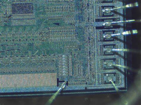
Reverse Microcontroller PIC12C508A structure and extract code from embedded mcu pic12c508a flash memory, decrypt the Firmware of pic12c508a microprocessor;
The clock recovery logic synchronizes internal clock to the incoming serial frames. Figure 87 illustrates the sampling process of the start bit of an incoming frame.
The sample rate is 16 times the baud rate for Normal mode, and eight times the baud rate for Double Speed mode. The horizontal arrows illustrate the synchronization variation due to the sampling process. Note the larger time variation when using the Double Speed mode (U2Xn = 1) of operation. Samples denoted zero are samples done when the RxDn line is idle (i.e., no communication activity).
Please shown in the figure. The clock recovery logic then uses samples 8, 9, and 10 for Normal mode, and samples 4, 5, and 6 for Double Speed mode (indicated with sample numbers inside boxes on the figure), to decide if a valid start bit is received.
If two or more of these three samples have logical high levels (the majority wins), the start bit is rejected as a noise spike and the Receiver starts looking for the next high to low-transition.
If however, a valid start bit is detected, the clock recovery logic is synchronized and the data recovery can begin. The synchronization process is repeated for each start bit before Breaking IC.
When the receiver clock is synchronized to the start bit, the data recovery can begin. The data recovery unit uses a state machine that has 16 states for each bit in Normal mode and eight states for each bit in Double Speed mode.
Figure 88 shows the sampling of the data bits and the parity bit. Each of the samples is given a number that is equal to the state of the recovery unit.The decision of the logic level of the received bit is taken by doing a majority voting of the logic value to the three samples in the center of the received bit when Restore IC program.
The center samples are emphasized on the figure by having the sample number inside boxes. The majority voting process is done as follows: If two or all three samples have high levels, the received bit is registered to be a logic 1.
If two or all three samples have low levels, the received bit is registered to be a logic 0. This majority voting process acts as a low pass filter for the incoming signal on the RxDn pin.
The recovery process is then repeated until a complete frame is received. Including the first stop bit. Note that the Receiver only uses the first stop bit of a frame.
Reverse Microcontroller ATmega8P Archive
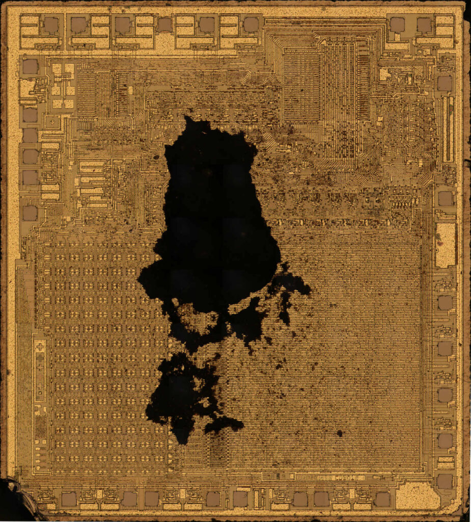
Reverse Microcontroller ATmega8P Archive needs to crack mcu atmega8p protective system and then extract locked code from mcu atmega8p flash memory;
The dashed boxes in the block diagram separate the three main parts of the USART (listed from the top): Clock Generator, Transmitter and Receiver.
Control Registers are shared by all units. The Clock Generation logic consists of synchronization logic for external clock input used by synchronous slave operation, and the baud rate generator if Recover atmega164pa MCU code.
The XCKn (Transfer Clock) pin is only used by synchronous transfer mode. The Transmitter consists of a single write buffer, a serial Shift Register, Parity Generator and Control logic for handling different serial frame formats.
The write buffer allows a continuous transfer of data without any delay between frames. The Receiver is the most complex part of the USART module due to its clock and data recovery units.
The recovery units are used for asynchronous data reception. In addition to the recovery units, the Receiver includes a Parity Checker, Control logic, a Shift Register and a two level receive buffer (UDRn).
The Receiver supports the same frame formats as the Transmitter, and can detect Frame Error, Data OverRun and Parity Errors if break microcontroller atmega324a binary.
The Clock Generation logic generates the base clock for the Transmitter and Receiver. The USARTn supports four modes of clock operation: Normal asynchronous, Double Speed asynchronous, Master synchronous and Slave synchronous mode.
The UMSELn bit in USART Control and Status Register C (UCSRnC) selects between asynchronous and synchronous operation. Double Speed (asynchronous mode only) is controlled by the U2Xn found in the UCSRnA Register.
When using synchronous mode (UMSELn = 1), the Data Direction Register for the XCKn pin (DDR_XCKn) controls whether the clock source is internal (Master mode) or external (Slave mode). The XCKn pin is only active when using synchronous mode.