 Break Microcontroller ATmega461A Firmware
 November 4th, 2010 |
  Author:
 The ATmega461A microcontroller is a high-performance, low-power 8-bit AVR RISC-based device widely relied upon in advanced battery charging systems, motor control peripherals, handheld power tools, and localized industrial sensor hubs. A standout feature of this chip is its highly flexible Pulse Width Modulation (PWM) channels paired with a high-speed Analog-to-Digital Converter, making it uniquely suited for precise analog regulation and high-frequency power management tasks. The core operating logic that directs these hardware operations runs silently as an embedded program within the chip’s internal structure. However, original equipment manufacturers frequently face critical production bottlenecks when a field system requires legacy optimization, but the development archives, original source code, or compiling records have been lost over time. When a component supplier disappears or a system faces immediate obsolescence, finding a reliable engineering path to extract the software becomes an absolute necessity. Our advanced laboratory specializes in precise engineering extractions designed to break microcontroller atmega461a firmware configurations, ensuring your business reclaims full operational access to its hardware investments.
The ATMEGA461A is a complex microcontroller with more peripheral units than can be supported within the 64 location reserved in the Opcode for the IN and OUT instructions.
For the Extended I/O space from $060 – $1FF in SRAM, only the ST/STS/STD and LD/LDS/LDD instructions can be used. The first 4,608/8,704 Data Memory locations address both the Register File, the I/O Memory, Extended I/O Memory, and the internal data SRAM. The first 32 locations address the Register file, the next 64 location the standard I/O Memory, then 416 locations of Extended I/O memory and the next 8,192 locations address the internal data SRAM. An optional external data SRAM can be used with the ATmega461. This SRAM will occupy an area in the remaining address locations in the 64K address space. This area starts at the address following the internal SRAM.
The Register file, I/O, Extended I/O and Internal SRAM occupies the lowest 4,608/8,704 bytes, so when using 64KB (65,536 bytes) of External Memory, 60,478/56,832 Bytes of External Memory are available. See “External Memory Interface” on page 29 for details on how to take advantage of the external memory map. When the addresses accessing the SRAM memory space exceeds the internal data memory locations, the external data SRAM is accessed using the same instructions as for the internal data memory access. When the internal data memories are accessed, the break and write strobe pins (PG0 and PG1) are inactive during the whole access cycle.
External SRAM operation is enabled by setting the SRE bit in the XMCRA Register. Accessing external SRAM takes one additional clock cycle per byte compared to access of the internal SRAM. This means that the commands LD, ST, LDS, STS, LDD, STD, PUSH, and POP take one additional clock cycle. If the Stack is placed in external SRAM, interrupts, subroutine calls and returns take three clock cycles extra because the three-byte program counter is pushed and popped, and external memory access does not take advantage of the internal pipe-line memory access.
When external SRAM interface is used with wait-state, one-byte external access takes two, three, or four additional clock cycles for one, two, and three wait-states respectively. Interrupts, subroutine calls and returns will need five, seven, or nine clock cycles more than specified in the instruction set manual for one, two, and three wait-states. The five different addressing modes for the data memory cover: Direct, Indirect with Displacement, Indirect, Indirect with Pre-decrement, and Indirect with Post-increment. In the Register file, registers R26 to R31 feature the indirect addressing pointer registers. The direct addressing reaches the entire data space. The Indirect with Displacement mode reaches 63 address locations from the base address given by the Y- or Z-register. When using register indirect addressing modes with automatic pre-decrement and post increment, the address registers X, Y, and Z are decremented or incremented.
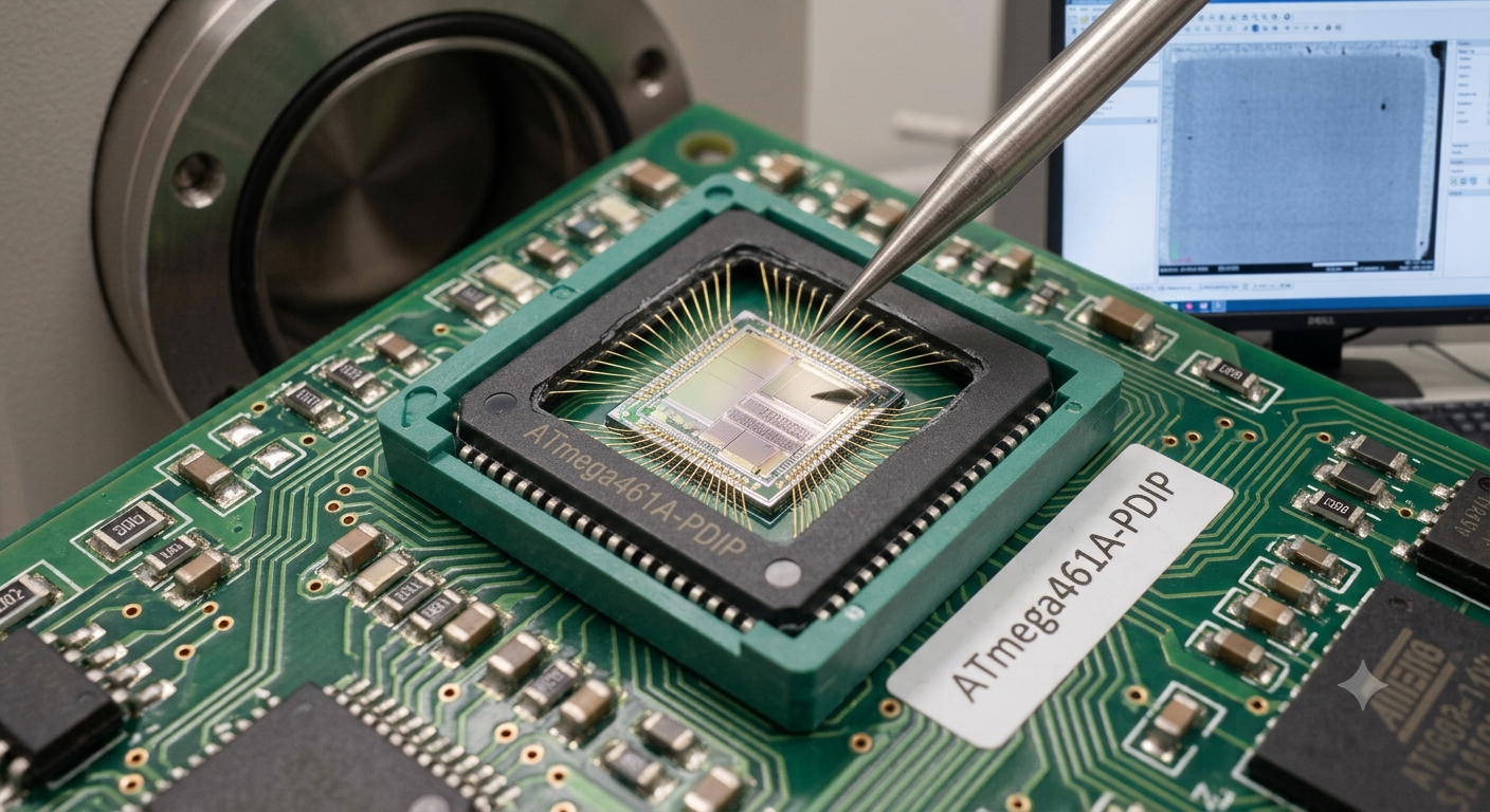
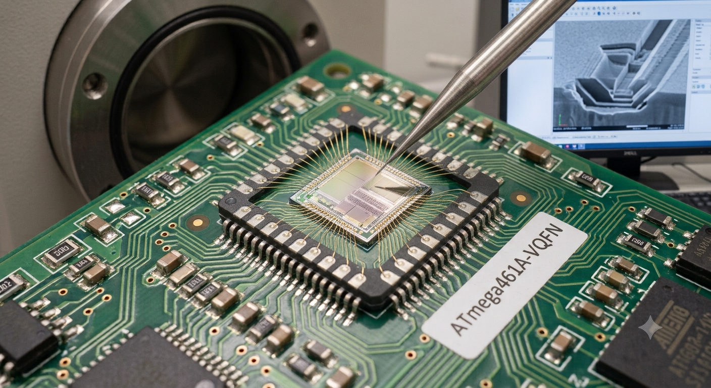
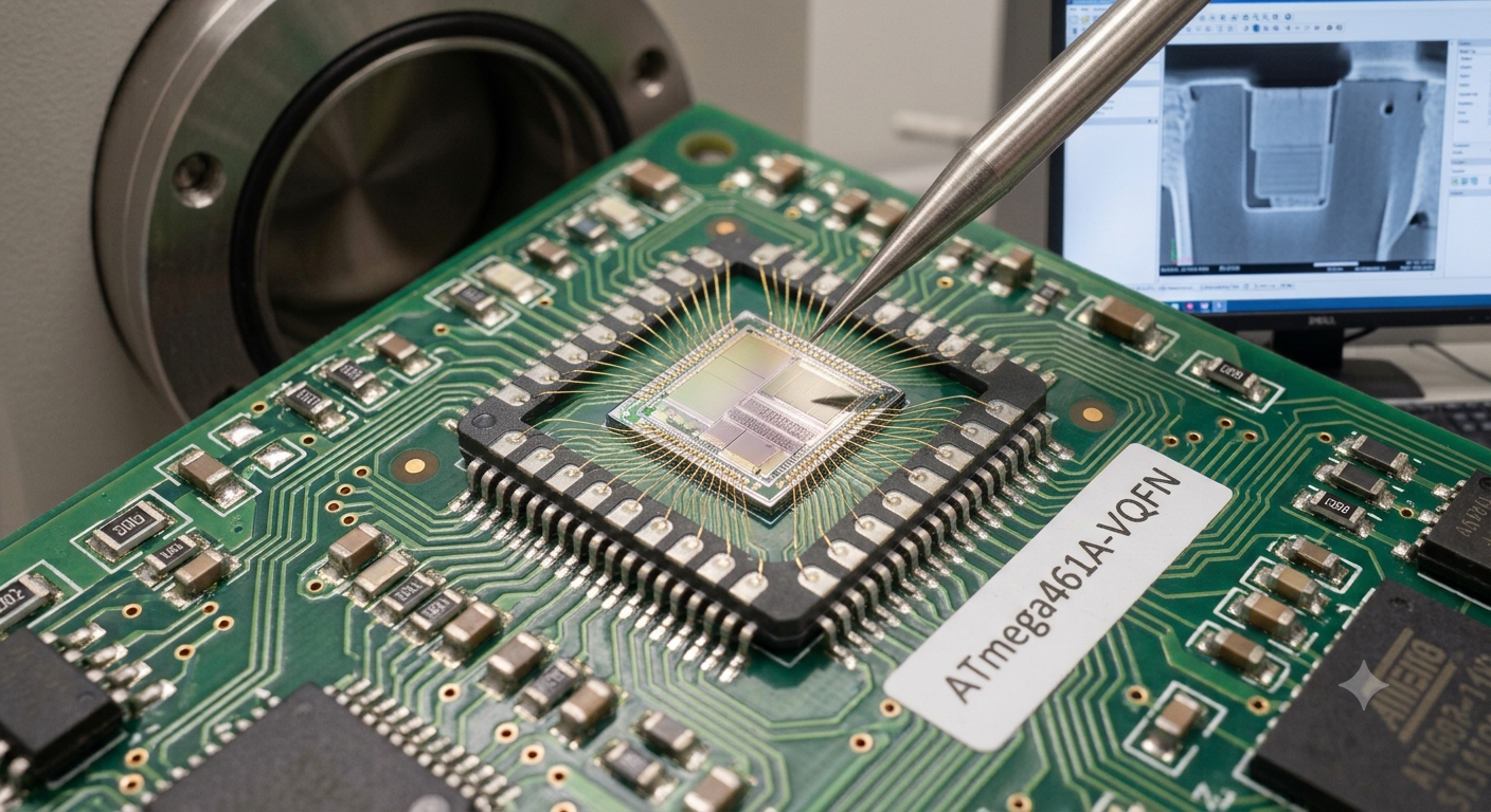
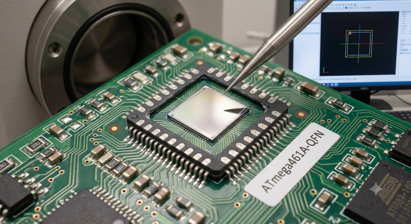
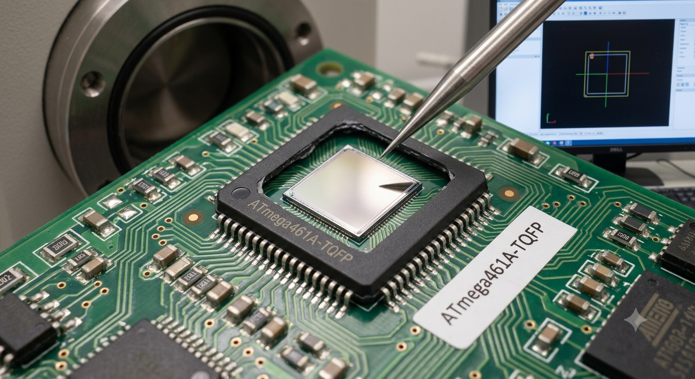
Accessing the machine instructions stored inside a secured or locked integrated circuit requires navigating dense physical and electrical defense systems designed to prevent unauthorized readout. To systematically attack, break, and decode these embedded protection mechanisms, our micro-electronics laboratory utilizes a non-destructive, highly controlled physical process. Technicians first decapsulate the outer protective plastic housing of the device using precise chemical etching to expose the raw silicon micro-die underneath. Once the internal circuitry is completely visible under high-power microscopy, we deploy specialized fault-injection and micro-probing equipment to target the protective code fuses and lock bits. By temporarily manipulating internal voltage levels or modifying configuration paths directly on the silicon substrate, our team can safely bypass the chip’s reading restrictions without destroying the underlying hardware. This allows us to smoothly retrieve the tightly guarded firmware, raw data, and structural configurations straight from the inner flash and internal eeprom memory sectors, compiling the extracted information into a flawless, uncorrupted heximal file that mirrors the original application instructions perfectly.
Eliminating Obsolescence Risks Through Precision Device Cloning
The underlying purpose of choosing to hack, duplicate, or extract code from a protected microcontroller is to insulate an enterprise from single-point supply chain failures and eliminate the massive costs of a ground-up software rewrite. When access to an active product file or software archive is severed, engineering teams use our advanced recovery services to salvage the vital logic required to clone the hardware’s exact operational profile. Whether the proprietary routines are held entirely in the main chip memory or distributed across peripheral PLD blocks, our custom extraction tools pull every byte of information safely. Once our team successfully extracts the raw data stream, developers gain the immediate capability to duplicate the system behavior onto a modern, readily available replacement microcontroller. This comprehensive recovery ensures you can maintain absolute system continuity, compile a fresh software backup, and confidently manufacture drop-in replacement boards without experiencing unexpected field downtime or production halts.
Strategic Capital Protection and Operational Benefits for the End User
Partnering with an experienced engineering team to unlock and recover embedded software gives product managers, system integrators, and maintenance engineers an immense technical and financial advantage. Instead of dedicating months of expensive R&D time to manually reverse-engineer and re-code a complex application from scratch—a risky process that notoriously introduces hidden programming bugs—our laboratory provides an efficient pipeline to a fully verified, operational firmware file. This absolute structural continuity guarantees that every newly generated duplicate circuit board performs identically to the field-proven units your customers already trust. By utilizing our custom microcontroller extraction services, your business effectively mitigates the existential risks of parts obsolescence, safeguards vital corporate intellectual property, and secures a completely predictable, stable roadmap for your industrial hardware investments for many years to come.
 Posted in Break IC