Archive for August, 2010
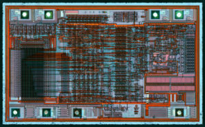
 Reverse Engineering Microcontroller ATtiny85 Flash
Reverse Engineering Microcontroller ATtiny85 is able to locate the fuse bit of attiny85 then unlock the mcu attiny85 by focus ion beam, program of Flash memory will be readout directly from mcu attiny85;
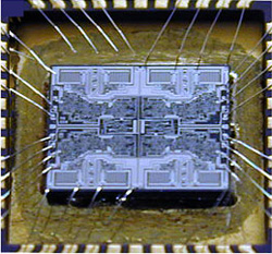
Reverse Engineering Microcontroller ATtiny85 is able to locate the fuse bit of attiny85 then unlock the mcu attiny85 by focus ion beam, program of Flash memory will be readout directly from mcu attiny85
The AVR core combines a rich instruction set with 32 general purpose working registers. All the 32 registers are directly connected to the Arithmetic Logic Unit (ALU), allowing two independent registers to be accessed in one single instruction executed in one clock cycle when Recover mcu pic12ce518 bin.
The resulting architecture is more code efficient while achieving throughputs up to ten times faster than conventional CISC microcontrollers. The ATtiny24/44/84 provides the following features: 2/4/8K byte of In-System Programmable Flash, 128/256/512 bytes EEPROM, 128/256/512 bytes SRAM, 12 general purpose I/O lines, 32 general purpose working registers, a 8-bit Timer/Counter with two PWM channels, a 16-bit timer/counter with two PWM channels, Internal and External Interrupts, a 8-channel 10-bit ADC, programmable gain stage (1x, 20x) for 12 differential ADC channel pairs, a programmable Watchdog Timer with internal Oscillator, internal calibrated oscillator, and three software selectable power saving modes.
The Idle mode stops the CPU while allowing the SRAM, Timer/Counter, ADC, Analog Comparator, and Interrupt system to continue functioning. The Power-down mode saves the register contents, disabling all chip functions until the next Interrupt or Hardware Reset. The ADC Noise Reduction mode stops the CPU and all I/O modules except ADC, to minimize switching noise during ADC conversions. In Standby mode, the crystal/resonator Oscillator is running while the rest of the device is sleeping. This allows very fast start-up combined with low power consumption before Reverse engineering Microcontroller.
The device is manufactured ng Atmel’s high density non-volatile memory technology. The On-chip ISP Flash allows the Program memory to be re-programmed In-System through an SPI serial interface, by a conventional non-volatile memory programmer or by an On-chip boot code running on the AVR core. The ATtiny24/44/84 AVR is supported with a full suite of program and system development tools including: C Compilers, Macro Assemblers, Program Debugger/Simulators, In-Circuit Emulators, and Evaluation kits if Reverse engineering Microcontroller.
Attack CPLD XC9536XL-10VQG44C Software
Attack CPLD XC9536XL-10VQG44C and disable the protection of CPLD, copy CPLD XC9536XL program from memory, JED Software will be extracted from CPLD IC chip memory;
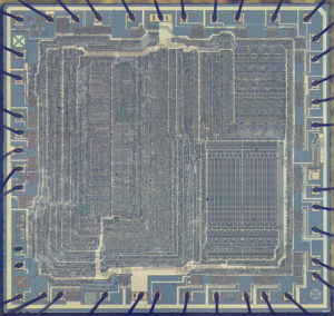
Attack CPLD XC9536XL-10VQG44C and disable the protection of CPLD, copy CPLD XC9536XL program from memory, JED Software will be extracted from CPLD IC chip memory
We can Attack CPLD XC9536XL-10VQG44C Software, please view below CPLD XC9536XL-10VQG44C features for your reference:
Features
· 5 ns pin-to-pin logic delays
· System frequency up to 178 MHz
Product Specification
54V18 Function Blocks, providing 800 usable gates with propagation delays of 5 ns. See Figure 2 for architecture overview when copy pic16f84a memory binary.
36 macrocells with 800 usable gates
Available in small footprint packages
– 44-pin PLCC (34 user I/O pins)
– 44-pin VQFP (34 user I/O pins)
– 48-pin CSP (36 user I/O pins)
– 64-pin VQFP (36 user I/O pins)
– Pb-free available for all packages
Optimized for high-performance 3.3V systems
– Low power operation
– 5V tolerant I/O pins accept 5 V, 3.3V, and 2.5V signals
– 3.3V or 2.5V output capability
– Advanced 0.35 micron feature size CMOS Fast FLASH™ technology
Advanced system features
– In-system programmable
– Superior pin-locking and routability with
Fast CONNECT™ II switch matrix
– Extra wide 54-input Function Blocks
– Up to 90 product-terms per macrocell with individual product-term allocation
– Local clock inversion with three global and one product-term clocks
– Individual output enable per output pin
– Input hysteresis on all user and boundary-scan pin inputs
– Bus-hold circuitry on all user pin inputs
– Full IEEE Standard 1149.1 boundary-scan (JTAG)
Fast concurrent programming
Slew rate control on individual outputs
Enhanced data security features
Excellent quality and reliability after Attack IC C8051F530 firmware
– Endurance exceeding 10,000 program/erase cycles
– 20 year data retention
– ESD protection exceeding 2,000V
Pin-compatible with 5V-core XC9536 device in the
Power Estimation
Power dissipation in CPLDs can vary substantially depending on the system frequency, design application and output loading when Attack CPLD. To help reduce power dissipation, each macrocell in a XC9500XL device may be configured for low-power mode (from the default high-performance mode).
In addition, unused product-terms and macrocells are automatically deactivated by the software to further conserve power.
For a general estimate of ICC, the following equation may be used:
ICC(mA) = MCHS(0.175*PTHS + 0.345) + MCLP(0.052*PTLP + 0.272) + 0.04 * MCTOG(MCHS +MCLP)* where if Attack CPLD:
MCHS = # macrocells in high-speed configuration
PTHS = average number of high-speed product terms per macrocell
MCLP = # macrocells in low power configuration
PTLP = average number of low power product terms per macrocell
f = maximum clock frequency before BREAK IC
MCTOG = average % of flip-flops toggling per clock (~12%)
This calculation was derived from laboratory measurements of an XC9500XL part filled with 16-bit counters and allowing
a single output (the LSB) to be enabled. The actual ICC value varies with the design application and should be verified during normal system operation. Figure 1 shows the above estimation in a graphical form. For a more detailed discussion of power consumption in this device, see Xilinx 44-pin PLCC package and the 48-pin CSP package.
WARNING: Programming temperature range of TA = 0° C to +70° C
Description
The XC9536XL is a 3.3V CPLD targeted for high-performance, low-voltage applications in leading-edge communications and computing systems.
Recover MCU ATtiny45V Program
Recover MCU ATtiny45V Program from flash and eeprom memory, unlock microcontroller attiny45v protection and readout beximal from mcu attiny45v memory;
Recover MCU ATtiny45V Program from flash and eeprom memory, unlock microcontroller attiny45v protection and readout beximal from mcu attiny45v memory
Port B is a 6-bit bi-directional I/O port with internal pull-up resistors (selected for each bit). The Port B output buffers have symmetrical drive characteristics with both high sink and source capability. As inputs, Port B pins that are externally pulled low will source current if the pull-up resistors are activated.
The Port B pins are tri-stated when a reset condition becomes active, even if the clock is not running. Reset input. A low level on this pin for longer than the minimum pulse length will generate a reset, even if the clock is not running. The minimum pulse length is given in Table 23-3 on page
170. Shorter pulses are not guaranteed to generate a reset.
A comprehensive set of development tools, application notes and datasheets are available for download on:
For compatibility with future devices, reserved bits should be written to zero if accessed. Reserved I/O memory addresses should never be written.
I/O Registers within the address range 0x00 – 0x1F are directly bit-accessible using the SBI and CBI instructions. In these registers, the value of single bits can be checked by using the SBIS and SBIC instructions.
Some of the Status Flags are cleared by writing a logical one to them. Note that, unlike most other AVRs, the CBI and SBI instructions will only operation the specified bit, and can therefore be used on registers containing such Status Flags. The CBI and SBI instructions work with registers 0x00 to 0x1F only.
PLL not locking
EEPROM recover from application code does not work in Lock Bit Mode 3
Recovering EEPROM at low frequency may not work for frequencies below 900 kHz Timer Counter 1 PWM output generation on OC1B- XOC1B does not work correctly, PLL not locking
When at frequencies below 6.0 MHz, the PLL will not lock
Problem fix / Workaround
When using the PLL, run at 6.0 MHz or higher.
EEPROM recover from application code does not work in Lock Bit Mode 3
When the Memory Lock Bits LB2 and LB1 are programmed to mode 3, EEPROM recover does not work from the application code.
Problem Fix/Work around
Do not set Lock Bit Protection Mode 3 when the application code needs to recover from EEPROM.
Recovering EEPROM at low frequency may not work for frequencies below 900 kHz, Recovering data from the EEPROM at low internal clock frequency may result in wrong data recover.
Problem Fix/Workaround
Avoid using the EEPROM at clock frequency below 900kHz. Timer Counter 1 PWM output generation on OC1B – XOC1B does not work correctly
Timer Counter1 PWM output OC1B-XOC1B does not work correctly. Only in the case when the control bits, COM1B1 and COM1B0 are in the same mode as COM1A1 and COM1A0, respectively, the OC1B-XOC1B output works correctly.
Problem Fix/Work around
The only workaround is to use same control setting on COM1A(1:0) and COM1B(1:0) control bits, see table 14-4 in the data sheet. The problem has been fixed for Tiny45 rev D.
Break PLD PALCE16V8H-15JC Software
Break PLD PALCE16V8H-15JC and extract Software from PALCE16V8 pld memory, copy JED file to new PLD chip;
We can Break PLD PALCE16V8H-15JC Software, please view below PLD PALCE16V8H-15JC features for your reference:
DISTINCTIVE CHARACTERISTICS
Pin and function compatible with all 20-pin GAL devices
Electrically erasable CMOS technology provides reconfigurable logic and full testability
High-speed CMOS technology
— 5-ns propagation delay for “-5” version
— 7.5-ns propagation delay for “-7” version
Direct plug-in replacement for the PAL16R8 series and most of the PAL10H8 series
Outputs programmable as registered or combinatorial in any combination, Peripheral Component Interconnect (PCI) compliant if recover pic16c554 software
GENERAL DESCRIPTION
The PALCE16V8 is an advanced PAL device built with low-power, high-speed, electrically-erasable CMOS technology. It is functionally compatible with all 20-pin GAL devices. The macrocells provide a universal device architecture.
The PALCE16V8 will directly replace the PAL16R8 and PAL10H8 series devices, with the excep-
tion of the PAL16C1.
The PALCE16V8 utilizes the familiar sum-of-products (AND/OR) architecture that allows users to implement complex logic functions easily and efficiently. Multiple levels of combinatorial logic can always be reduced to sum-of-products form, taking advantage of the very wide input gates available in PAL devices after recover microcontroller pic16f83 eeprom.
The equations are programmed into the device through floating gate cells in the AND logic array that can be erased electrically.
Programmable output polarity
Programmable enable/disable control
Preloadable output registers for testability
Automatic register reset on power up
Cost-effective 20-pin plastic DIP, PLCC, and SOIC packages
Extensive third-party software and programmer support through FusionPLD partners
Fully tested for 100% programming and functional yields and high reliability
5 ns version utilizes a split leadframe for improved performance.
The fixed OR array allows up to eight data product terms per output for logic functions. The sum of these products feeds the output macrocell. Each macrocell can be programmed as registered or combinatorial with an active high or active-low output after Break EPM3128ATC100 CPLD.
The output configuration is determined by two global bits and one local bit controlling four multiplexers in each macrocell.
AMD’s FusionPLD program allows PALCE16V8 designs to be implemented using a wide variety of popular industry-standard design tools. By working closely with the FusionPLD partners, AMD certifies that the tools provide accurate, quality support.
By ensuring that third party tools are available, costs are lowered because a designer does not have to buy a complete set of new tools for each device. The Fusion PLD program also greatly reduces design time since a designer can use a tool that is already installed and familiar.
Break IC ATtiny45 Heximal
Break IC ATtiny45 and readout Heximal from mcu attiny45 flash memory, unlock microcontroller attiny45 security fuse bit and remove the protection;
Port B is a 6-bit bi-directional I/O port with internal pull-up resistors (selected for each bit). The Port B output buffers have symmetrical drive characteristics with both high sink and source capability. As inputs, Port B pins that are externally pulled low will source current if the pull-up resistors are activated.
The Port B pins are tri-stated when a reset condition becomes active, even if the clock is not running. Reset input. A low level on this pin for longer than the minimum pulse length will generate a reset, even if the clock is not running.
The minimum pulse length is given in Table 23-3 on page 170. Shorter pulses are not guaranteed to generate a reset. For compatibility with future devices, reserved bits should be written to zero if accessed. Reserved I/O memory addresses should never be written. I/O Registers within the address range 0x00 – 0x1F are directly bit-accessible using the SBI and CBI instructions. In these registers, the value of single bits can be checked by using the SBIS and SBIC instructions when Break pic16f616 IC.
Some of the Status Flags are cleared by writing a logical one to them. Note that, unlike most other AVRs, the CBI and SBI instructions will only operation the specified bit, and can therefore be used on registers containing such Status Flags. The CBI and SBI instructions work with registers 0x00 to 0x1F only.
The ATTINY45 provides the following standard features:
20K bytes of Flash, 256-bytes of RAM, 32 I/O lines, three 16-bit timer/counters, a six-vector two-level interrupt architecture, a full duplex serial port, on-chip oscillator, and clock circuitry. In addition, the AT89C55 is designed with static logic for operation down to zero frequency and supports two software selectable power saving modes.
The Idle Mode stops the CPU while allowing the RAM, timer/counters, serial port, and interrupt system to continue functioning. The Power Down Mode saves the RAM contents but freezes the oscillator, disabling all other chip functions until the next hardware reset. The low-voltage option saves power and operates with a 2.7-volt power supply if Break IC.
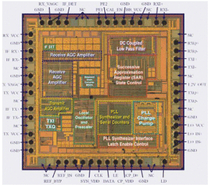
Recover CPLD CY37256VP160-100AC Binary
We can Recover CPLD CY37256VP160-100AC Binary, please view below CPLD CY37256VP160-100AC features for your reference:
Features
· In-System Reprogrammable™ (ISR™) CMOS CPLDs
— JTAG interface for reconfigurability
— Design changes do not cause pinout changes
— Design changes do not cause timing changes when Recover CPLD
· High density
— 32 to 512 macrocells
— 32 to 264 I/O pins
— Five dedicated inputs including four clock pins
· Simple timing model
— No fanout delays
— No expander delays
— No dedicated vs. I/O pin delays
— No additional delay through PIM
— No penalty for using full 16 product terms
— No delay for steering or sharing product terms if Recover CPLD
General Description
The Ultra37000™ family of CMOS CPLDs provides a range of high-density programmable logic solutions with unparalleled
system performance. The Ultra37000 family is designed to bring the flexibility, ease of use, and performance of the 22V10 after Recover CPLD
to high-density CPLDs. The architecture is based on a number of logic blocks that are connected by a Programmable Inter-
connect Matrix (PIM). Each logic block features its own product term array, product term allocator, and 16 macrocells.
The PIM distributes signals from the logic block outputs and all input pins to the logic block inputs before Recover CPLD.
All of the Ultra37000 devices are electrically erasable and In-System Reprogrammable (ISR), which simplifies both design
and manufacturing flows, thereby reducing costs. The ISR feature provides the ability to reconfigure the devices without
having design changes cause pinout or timing changes. The Cypress ISR function is implemented through a JTAG-compliant serial interface. Data is shifted in and out through the TDI and TDO pins, respectively. Because of the superior routability and simple timing model of the Ultra37000 devices, ISR allows users to change existing logic designs while simultaneously fixing pinout assignments and maintaining system performance when Recover CPLD.
3.3V and 5V versions
PCI-compatible[1]
Programmable bus-hold capabilities on all I/Os
Intelligent product term allocator provides:
— 0 to 16 product terms to any macrocell before Recover CPLD
The entire family features JTAG for ISR and boundary scan, and is compatible with the PCI Local Bus specification,
meeting the electrical and timing requirements. The Ultra37000 family features user programmable bus-hold capabilities on all I/Os.
— Product term steering on an individual basis after Recover CPLD
— Product term sharing among local macrocells
· Flexible clocking
— Four synchronous clocks per device
— Product term clocking
— Clock polarity control per logic block
· Consistent package/pinout offering across all densities
— Simplifies design migration
— Same pinout for 3.3V and 5.0V devices if Recover MCU
· Packages
— 44 to 400 leads in PLCC, CLCC, PQFP, TQFP, CQFP,
BGA, and Fine-Pitch BGA packages
Ultra37000 5.0V Devices
The Ultra37000 devices operate with a 5V supply and can support 5V or 3.3V I/O levels. VCCO connections provide the
capability of interfacing to either a 5V or 3.3V bus. By connecting the VCCO pins to 5V the user insures 5V TTL levels on the outputs. If VCCO is connected to 3.3V the output levels meet 3.3V JEDEC standard CMOS levels and are 5V tolerant when Recover CPLD.
These devices require 5V ISR programming.
Ultra37000V 3.3V Devices
Devices operating with a 3.3V supply require 3.3V on all VCCO pins, reducing the device’s power consumption. These devices support 3.3V JEDEC standard CMOS output levels, and are 5V-tolerant. These devices allow 3.3V ISR programming before Recover CPLD.