Posts Tagged ‘break mcu encrypted data’
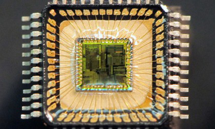
 Break MCU PIC16F631 Flash
When a device depends on the Microchip PIC16F631 for control, timing, or sensor interfacing, loss of access to on-chip flash or EEPROM can stop equipment and erase critical calibration data. Our service, indexed as Break MCU PIC16F631 Flash, helps legitimate owners and authorized technicians open, readout, restore, and duplicate the embedded firmware/binary/heximal images stored in these controllers. We focus on safe, lawful recovery that returns usable program archives without revealing methods to crack, hack, or bypass protections.
Clients commonly need us to restore corrupted files, copy firmware for authorized spares, clone settings for production, or duplicate configuration archives before servicing legacy systems. Devices using the PIC16F631 often contain small but vital pieces of source code, calibration tables and settings in flash or EEPROM — assets that, when protected, may be inaccessible without professional, authorized support.
We can Break MCU PIC16F685 flash, please view the MCU PIC16F685 features for your reference:
High-Performance RISC CPU:
· Only 35 instructions to learn:
– All single-cycle instructions except branches
The PIC16F631’s compact footprint and mixed-signal capabilities make it a frequent choice across many industries:
- Consumer electronics and appliance controllers.
- Industrial sensors and simple automation modules.
- Instrumentation and small test equipment.
- Aftermarket automotive modules and hobbyist/legacy embedded systems.
Because these applications store operational data and program archives on the device, being able to recover a verified binary or heximal dump can be essential to restore service quickly.
· Operating speed:
– DC – 20 MHz oscillator/clock input
– DC – 200 ns instruction cycle
· Interrupt capability
· 8-level deep hardware stack
· Direct, Indirect and Relative Addressing modes
Special Microcontroller Features:
· Precision Internal Oscillator:
– Factory calibrated to ± 1%
– Software selectable frequency range of 8 MHz to 32 kHz
– Software tunable
– Two-Speed Start-up mode
– Crystal fail detect for critical applications
– Clock mode switching during operation for power savings
· Power-Saving Sleep mode
· Wide operating voltage range (2.0V-5.5V)
· Industrial and Extended Temperature range
· Power-on Reset (POR)
· Power-up Timer (PWRTE) and Oscillator Start-up Timer (OST)
· Brown-out Reset (BOR) with software control option and for MCU reading
· Enhanced low-current Watchdog Timer (WDT) with on-chip oscillator (software selectable nominal 268 seconds with full prescaler) with software enable
· Multiplexed Master Clear/Input pin
· Programmable code protection
· High Endurance Flash/EEPROM cell:
– 100,000 write Flash endurance
– 1,000,000 write EEPROM endurance
– Flash/Data EEPROM retention: > 40 years
· Enhanced USART module:
– Supports RS-485, RS-232 and LIN 2.0
– Auto-Baud Detect
– Auto-wake-up on Start bit
The PIC16F631 integrates modest program flash, EEPROM, and analog/digital peripherals in a tight package. Its memory layout concentrates configuration and calibration data in discrete regions, and many designs set protective or locked configurations to prevent unauthorized copying. Those features shape how a lawful recovery is scoped and the kinds of deliverables that best serve the end user.
What we provide (high level, non-actionable)
Our engagements emphasize ethical, non-destructive recovery. Typical deliverables include validated binary/heximal dumps of flash and EEPROM where permitted, integrity and checksum reports, and high-level annotated summaries that help engineers interpret recovered program logic. We can assist clients to restore devices to operation using recovered files, prepare migration packages for replacement hardware, and advise on safe duplication and archival strategies. Importantly, we do not publish or provide step-by-step instructions to decrypt, unlock, or otherwise compromise manufacturer protections.
Conceptual approach and purpose
A responsible recovery project begins with verification of ownership and a feasibility assessment. The objective is to obtain a reliable memory archive and translate raw data into a usable representation for maintenance, testing, or authorized redevelopment. The primary purposes are to reduce downtime, secure previously inaccessible firmware, and enable legitimate copying or cloning for spares and production.
Benefits for the end user
Clients benefit from secure backups of embedded firmware and data, faster restoration of equipment, and the ability to duplicate or deploy authorized copies across installations. Recovered program archives reduce the need to rebuild software from scratch and protect investment in specialized hardware.
Challenges and limitations
Obstacles can include layered protective settings, partial memory corruption, variant device revisions, and proprietary integrity checks. Full source-level reconstruction is not always possible; often the practical outcome is a validated heximal or binary archive with assembly-level annotations. We communicate feasibility and likely outcomes before proceeding.
Legal & ethical safeguards
All projects require explicit authorization and operate under confidentiality agreements. Our mission is to help rightful owners recover, restore, and preserve their embedded systems for lawful, constructive purposes only.
If you need to Break MCU PIC16F631 Flash for authorized recovery, maintenance, or archival purposes, our experienced team provides confidential, professional support to retrieve and document your embedded program and data while protecting your IP and operational continuity.
Break MCU ATmega128PA Heximal
Break MCU ATmega128APA flash memory and readout chip ATmega128PA content inside it in the format of Heximal, the code can be reprogrammed to new ATmega128PA microcontroller for cloning;
OC1A/PCINT5, Bit 5
OC1A, Output Compare Match A output: The PB5 pin can serve as an external output for the Timer/Counter1 Output Compare A. The pin has to be configured as an output (DDB5 set (one)) to serve this function. The OC1A pin is also the output pin for the PWM mode timer function.
PCINT5, Pin Change Interrupt source 5: The PB7 pin can serve as an external interrupt source.
OC2A/PCINT4, Bit 4
OC2A, Output Compare Match output: The PB4 pin can serve as an external output for the Timer/Counter2 Output Compare. The pin has to be configured as an output (DDB4 set (one)) to serve this function. The OC2A pin is also the output pin for the PWM mode timer function when recover mcu pic16c554 software.
PCINT4, Pin Change Interrupt source 4: The PB7 pin can serve as an external interrupt source.
MISO/PCINT3 – Port B, Bit 3
MISO: Master Data input, Slave Data output pin for SPI channel. When the SPI is enabled as a master, this pin is configured as an input regardless of the setting of DDB3. When the SPI is enabled as a slave, the data direction of this pin is controlled by DDB3. When the pin is forced to be an input, the pull-up can still be controlled by the PORTB3 bit.
PCINT3, Pin Change Interrupt source 3: The PB7 pin can serve as an external interrupt source when Break MCU heximal.
MOSI/PCINT2 – Port B, Bit 2
MOSI: SPI Master Data output, Slave Data input for SPI channel. When the SPI is enabled as a slave, this pin is configured as an input regardless of the setting of DDB2. When the SPI is enabled as a master, the data direction of this pin is controlled by DDB2. When the pin is forced to be an input, the pull-up can still be controlled by the PORTB2 bit.
PCINT2, Pin Change Interrupt source 2: The PB7 pin can serve as an external interrupt source.
SCK/PCINT1 – Port B, Bit 1
SCK: Master Clock output, Slave Clock input pin for SPI channel. When the SPI is enabled as a slave, this pin is configured as an input regardless of the setting of DDB1. When the SPI0 is enabled as a master, the data direction of this pin is controlled by DDB1. When the pin is forced to be an input, the pull-up can still be controlled by the PORTB1 bit.
PCINT1, Pin Change Interrupt source 1: The PB7 pin can serve as an external interrupt source.
Break MCU ATtiny24V Flash
Break MCU ATtiny24V security fuse bit and crack microcontroller attiny24v system against unauthorized reading, extract program from attiny24v mcu Flash and eeprom memory;
The AVR core combines a rich instruction set with 32 general purpose working registers. All the 32 registers are directly connected to the Arithmetic Logic Unit (ALU), allowing two independent registers to be accessed in one single instruction executed in one clock cycle when Break pld palce16v8 software.
The resulting architecture is more code efficient while achieving throughputs up to ten times faster than conventional CISC mcus.
The ATtiny24/44/84 provides the following features: 2/4/8K byte of In-System Programmable Flash, 128/256/512 bytes EEPROM, 128/256/512 bytes SRAM, 12 general purpose I/O lines, 32 general purpose working registers, a 8-bit Timer/Counter with two PWM channels, a 16-bit timer/counter with two PWM channels, Internal and External Interrupts, a 8-channel 10-bit ADC, programmable gain stage (1x, 20x) for 12 differential ADC channel pairs, a programmable Watchdog Timer with internal Oscillator, internal calibrated oscillator, and three software selectable power saving modes if Break pic16c717 mcu program.
The Idle mode stops the CPU while allowing the SRAM, Timer/Counter, ADC, Analog Comparator, and Interrupt system to continue functioning. The Power-down mode saves the register contents, disabling all chip functions until the next Interrupt or Hardware Reset before attack pic16c710 Mcu.
The ADC Noise Reduction mode stops the CPU and all I/O modules except ADC, to minimize switching noise during ADC conversions. In Standby mode, the crystal/resonator Oscillator is running while the rest of the device is sleeping. This allows very fast start-up combined with low power consumption.
The device is manufactured ng Atmel’s high density non-volatile memory technology. The On-chip ISP Flash allows the Program memory to be re-programmed In-System through an SPI serial interface, by a conventional non-volatile memory programmer or by an On-chip boot code running on the AVR core.
The ATtiny24/44/84 AVR is supported with a full suite of program and system development tools including: C Compilers, Macro Assemblers, Program Debugger/Simulators, In-Circuit Emulators, and Evaluation kits. Port B is a 4-bit bi-directional I/O port with internal pull-up resistors (selected for each bit) if recover pic16c74 Mcu code.
The Port B output buffers have symmetrical drive characteristics with both high sink and source capability except PB3 which has the RESET capability. To use pin PB3 as an I/O pin, instead of RESET pin, program (‘0’) RSTDISBL fuse. As inputs, Port B pins that are externally pulled low will source current if the pull-up resistors are activated.
The Port B pins are tri-stated when a reset condition becomes active, even if the clock is not running. Port A is a 8-bit bi-directional I/O port with internal pull-up resistors (selected for each bit). The Port A output buffers have symmetrical drive characteristics with both high sink and source capability.
As inputs, Port A pins that are externally pulled low will source current if the pull-up resistors are activated. The Port A pins are tri-stated when a reset condition becomes active, even if the clock is not running.
Break MCU ATmega64PA Binary
Break MCU ATmega64PA and readout the embedded Binary from microcontroller atmega64pa flash memory, fuse bit of mcu atmega64pa will be crack to disable the protection;
The ATmega64 is a highly complex mcu where the number of I/O locations supersedes the 64 I/O location reserved in the AVR instruction set. To ensure backward compatibility with the ATmega103, all I/O locations present in ATmega103 have the same location in ATmega64. Most additional I/O locations are added in an Extended I/O space starting from 0x60 to 0xFF (i.e., in the ATmega103 internal RAM space). These location can be reached by using LD/LDS/LDD and ST/STS/STD instructions only, not by using IN and OUT instructions. The relocation of the internal RAM space may still be a problem for ATmega103 users.
Also, the increased number of Interrupt Vectors might be a problem if the code uses absolute addresses. To solve these problems, an ATmega103 compatibility mode can be selected by programming the fuse M103C. In this mode, none of the functions in the Extended I/O space are in use, so the internal RAM is located as in ATmega103. Also, the extended Interrupt Vectors are removed. The ATmega64 is 100% pin compatible with ATmega103, and can replace the ATmega103 on current printed circuit boards. The application notes “Replacing ATmega103 by ATmega128” and “Migration between ATmega64 and ATmega128” describes what the user should be aware of replacing the ATmega103 by an ATmega128 or ATmega64PA.
By programming the M103C Fuse, the ATmega64 will be compatible with the ATmega103 regards to RAM, I/O pins and Interrupt Vectors as described above. However, some new features in ATmega64 are not available in this compatibility mode, these features are listed:
Pin Descriptions
One USART instead of two, asynchronous mode only. Only the eight least significant bits of the Baud Rate Register is available. One 16 bits Timer/Counter with two compare registers instead of two 16 bits Timer/Counters with three compare registers. Two-wire serial interface is not supported.
Port G serves alternate functions only (not a general I/O port). Port F serves as digital input only in addition to analog input to the ADC. Boot Loader capabilities is not supported. It is not possible to adjust the frequency of the internal calibrated RC Oscillator. The External Memory Interface can not release any Address pins for general I/O, neither configure different wait states to different External Memory Address sections. Only EXTRF and PORF exist in the MCUCSR Register. No timed sequence is required for Watchdog Timeout change. Only low-level external interrupts can be used on four of the eight External Interrupt sources. Port C is output only. USART has no FIFO buffer, so Data OverRun comes earlier. The user must have set unused I/O bits to 0 in ATmega103 programs after Break IC.