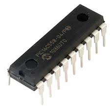
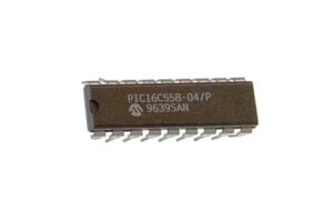
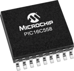
 Reverse Engineering Microcontroller PIC16C558A Eeprom
Microcontrollers like the PIC16C558A store critical firmware and data in their internal EEPROM, often under protective security measures to prevent unauthorized access. However, in various scenarios—such as legacy system recovery, security analysis, or system optimization—it becomes necessary to restore, decrypt, or duplicate the locked firmware for further use. We specialize in Reverse Engineering Microcontroller PIC16C558A EEPROM, offering professional solutions to decode and clone its embedded program.

Az olyan mikrokontrollerek, mint a PIC16C558A, a kritikus firmware-t és adatokat belső EEPROM-jukban tárolják, gyakran biztonsági intézkedések mellett, hogy megakadályozzák az illetéktelen hozzáférést. Különféle forgatókönyvek esetén azonban – például a régi rendszer-helyreállításban, biztonsági elemzésben vagy rendszeroptimalizálásban – szükségessé válik a zárolt firmware visszaállítása, visszafejtése vagy másolása a további használathoz. Szakterületünk a PIC16C558A EEPROM Reverse Engineering mikrokontroller, amely professzionális megoldásokat kínál a beágyazott program dekódolására és klónozására.
Unlocking Protected PIC16C558A EEPROM
The PIC16C558A EEPROM is designed with secured features to prevent unauthorized access, but our advanced firmware decryption and binary analysis techniques allow us to attack these security barriers and retrieve the original heximal source code. Using specialized hardware and software tools, we can copy, extract, and restore the flash memory, providing a complete binary file for modification or further study.

PIC16C558A EEPROM разработан с защищенными функциями для предотвращения несанкционированного доступа, но наши передовые методы дешифрования прошивки и двоичного анализа позволяют нам атаковать эти барьеры безопасности и извлекать исходный шестнадцатеричный код. Используя специализированные аппаратные и программные инструменты, мы можем копировать, извлекать и восстанавливать флэш-память, предоставляя полный двоичный файл для модификации или дальнейшего изучения.
Our Expertise in Microcontroller Hacking and Cloning
- EEPROM Data Extraction – We use cutting-edge techniques to unlock and decrypt the secured firmware stored in flash memory.
- Reverse Engineering & Decompilation – Our team converts binary code into readable source code, making it easier to analyze and modify.
- Firmware Duplication & Cloning – Whether you need to duplicate, clone, or open an archived program, we ensure high accuracy and reliability.
- Security Research & Debugging – Identifying vulnerabilities in protected microcontrollers is crucial for debugging and cybersecurity assessments.

Nossa experiência em hacking e clonagem de microcontroladores
Extração de dados EEPROM – Usamos técnicas de ponta para desbloquear e descriptografar o firmware protegido armazenado na memória flash.
Engenharia reversa e descompilação – Nossa equipe converte código binário em código-fonte legível, facilitando a análise e a modificação.
Duplicação e clonagem de firmware – Se você precisa duplicar, clonar ou abrir um programa arquivado, garantimos alta precisão e confiabilidade.
Pesquisa e depuração de segurança – Identificar vulnerabilidades em microcontroladores protegidos é crucial para avaliações de depuração e segurança cibernética.
Why Choose Us?
- Proven expertise in microcontroller reverse engineering
- Advanced tools for breaking encrypted EEPROM firmware
- Confidential and secure services tailored to client needs
At [Your Company Name], we help you crack, copy, and decrypt PIC16C558A EEPROM firmware with precision. Contact us today to discuss your project and recover valuable memory files from locked microcontrollers!
The clock input (OSC1/CLKIN pin) is internally divided by four to generate four non-overlapping quadrature clocks namely Q1, Q2, Q3 and Q4. Internally, the program counter (PC) is incremented every Q1 if Reverse Engineering Microcontroller PIC16C558A Eeprom, the instruction is fetched from the program memory and latched into the instruction register in Q4. The instruction is decoded and executed during the following Q1 through Q4..
An “Instruction Cycle” consists of four Q cycles (Q1, Q2, Q3 and Q4). The instruction fetch and execute are pipelined such that fetch takes one instruction cycle while decode and execute takes another instruction cycle similar to the process of Reverse Engineering Microcontroller PIC16F73 Program.

Reverse Engineering Microcontroller PIC16C558A Eeprom
However, due to the pipelining, each instruction effectively executes in one cycle. If an instruction causes the program counter to change (e.g., GOTO) then two cycles are required to complete the instruction (Example 3-1) after Reverse engineering Microcontroller. A fetch cycle begins with the program counter (PC) incrementing in Q1.
In the execution cycle, the fetched instruction is latched into the “Instruction Register (IR)” in cycle Q1. This instruction is then decoded and executed during the Q2, Q3, and Q4 cycles. Data memory is read during Q2 (operand read) and written during Q4 (destination write).
The PIC16C55X(A) has a 13-bit program counter capable of addressing an 8K x 14 program memory space. Only the first 512 x 14 (0000h – 01FFh) for the PIC16C554(A), 1K x 14 (0000h – 03FFh) for the PIC16C556A and 2K x 14 (0000h – 07FFh) for the PIC16C558(A) are physically implemented.
Accessing a location above these boundaries will cause a wrap-around within the first 512 x 14 space PIC16C554(A) or 1K x 14 space PIC16C556A or 2K x 14 space PIC16C558(A). The reset vector is at 0000h and the interrupt vector is at 0004h when Recover MCU PIC16F74A Binary.
The data memory (Figure 4-4 and Figure 4-5) is partitioned into two Banks which contain the general purpose registers and the special function registers. Bank 0 is selected when the RP0 bit is cleared. Bank 1 is selected when the RP0 bit (STATUS <5>) is set.
The Special Function Registers are located in the first 32 locations of each Bank. Register locations 20-6Fh (Bank0) on the PIC16C554(A)/556A and 20-7Fh (Bank0) and A0-BFh (Bank1) on the PIC16C558(A) are general purpose registers implemented as static RAM when Reverse Engineering Microcontroller PIC16C558A Eeprom. Some special purpose registers are mapped in Bank 1