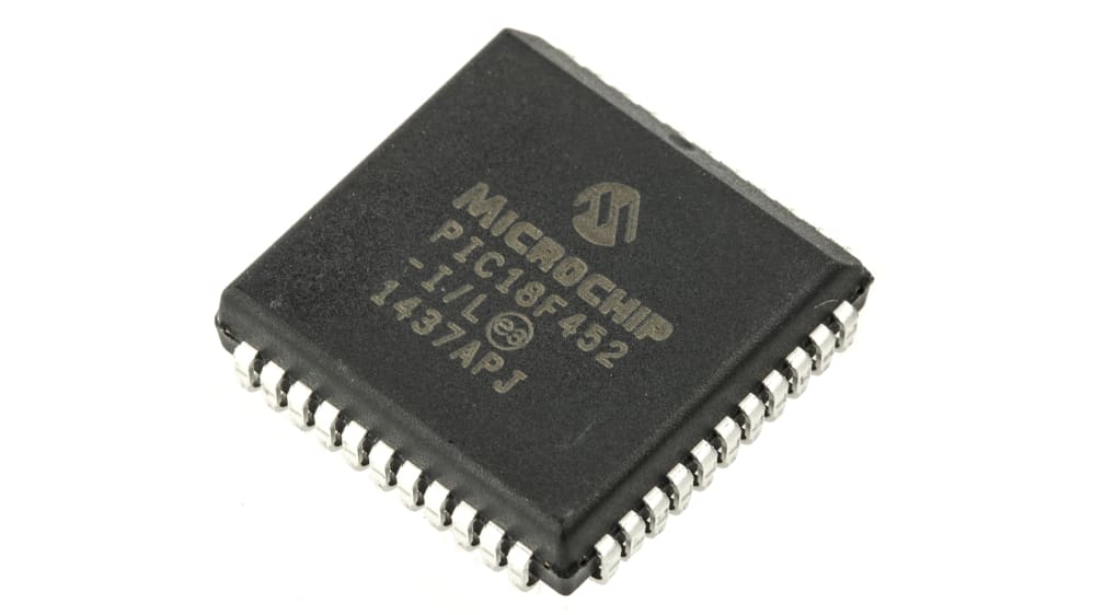
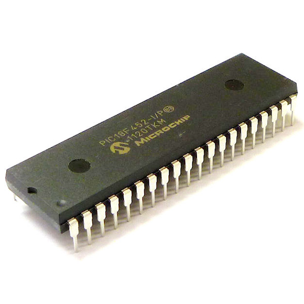
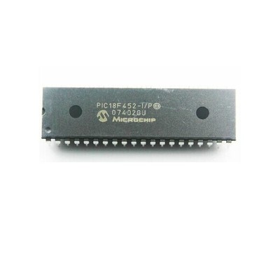
 Recover MCU PIC18F452 Program
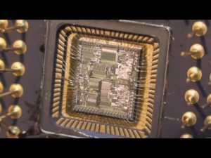
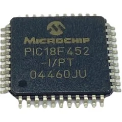
When embedded systems fail, are upgraded, or require inspection, access to the original firmware can be vital. Our service — summarized under the keyword Recover MCU PIC18F452 Program — helps legitimate owners and authorized technicians restore, readout, copy, clone, or duplicate the protected program held inside Microchip’s PIC18F452 MCU. We focus on recovering the firmware/binary/heximal image and producing usable outputs while respecting legal and ethical boundaries.
Recover MCU PIC18F452 Program starts from unlocking microcontroller pic18f452 secured memory and extract pic18f452 secured flash memory content;
A “fast interrupt return” option is available for interrupts. A Fast Register Stack is provided for the STATUS, WREG and BSR registers and are only one in depth. The stack is not recoverable or writable and is loaded with the current value of the corresponding register when the processor vectors for an interrupt. The values in the registers are then loaded back into the working registers, if the FAST RETURN instruction is used to return from the interrupt.
A low or high priority interrupt source will push values into the stack registers. If both low and high priority interrupts are enabled, the stack registers cannot be used reliably for low priority interrupts. If a high priority interrupt occurs while servicing a low priority interrupt, the stack register values stored by the low priority interrupt will be overwritten if break pic12f635 MCU program.
Why clients need PIC18F452 program recovery
The PIC18F452 is a workhorse in many legacy and modern applications thanks to its flexible I/O, analog and timing peripherals, and on-chip nonvolatile memories. Devices built around this MCU often contain essential program files, calibration data, and archived memory that control hardware behavior. Typical reasons to request recovery include:
- Restore a device after accidental corruption or bad firmware updates.
- Duplicate/clone firmware for manufacturing spares or supporting legacy production.
- Migrate software to replacement hardware during end-of-life transitions.
- Audit or validate embedded code for safety, compliance, or forensic analysis.
What we do (high level, non-invasive)
Our service helps customers to legally open, unlock, decode, and extract the embedded flash/eeprom contents without publishing methods to bypass manufacturer protections. Key outcomes include:
- Verified extraction of the raw binary/heximal firmware image.
- Data integrity checks and documented checksums for recovery traceability.
- High-level decoding and annotated disassembly to aid engineers in understanding the recovered code.
- Delivery of recoverable files and a concise recovery report describing what was found and recommended next steps.
We do not provide procedural guidance to circumvent protections for unlawful purposes. All projects require proof of ownership or explicit authorization.
If high priority interrupts are not disabled during low priority interrupts, users must save the key registers in software during a low priority interrupt. If no interrupts are used, the fast register stack can be used to restore the STATUS, WREG and BSR registers at the end of a subroutine call. To use the fast register stack for a subroutine call, a FAST CALL instruction must be executed.
Example 4-1 shows a source code example that uses the fast register stack. The program counter (PC) specifies the address of the instruction to fetch for execution. The PC is 21-bits wide. The low byte is called the PCL register. This register is recoverable and writable. The high byte is called the PCH register. This register contains the PC<15:8> bits and is not directly recoverable or writable after break pic12f629 MCU program.
Updates to the PCH register may be performed through the PCLATH register. The upper byte is called PCU. This register contains the PC<20:16> bits and is not directly recoverable or writable. Updates to the PCU register may be performed through the PCLATU register.
The PC addresses bytes in the program memory. To prevent the PC from becoming misaligned with word instructions, the LSB of PCL is fixed to a value of ’0’. The PC increments by 2 to address sequential instructions in the program memory.
The CALL, RCALL, GOTO and program branch instructions write to the program counter directly. For these instructions, the contents of PCLATH and PCLATU are not transferred to the program counter.
Applications where PIC18F452 matters
The PIC18F452’s blend of digital control and analog support makes it common across multiple industries:
- Industrial controllers and instrumentation, where deterministic timing and ADCs matter.
- Consumer electronics and appliances, for feature logic and user interfaces.
- Automotive subsystems in legacy modules that use robust 8-bit control.
- Medical instruments and test equipment that rely on stable, well-tested firmware.
Because these systems often run long past their original support window, firmware recovery is frequently the only path to safe maintenance, calibration, or legal continuity.
Unique recovery considerations for PIC18F452
The PIC18F family commonly stores program code in on-chip flash with supplementary EEPROM for parameter data. Firmware may be protected, locked, or use custom bootloader schemes that complicate straightforward readout. Our approach combines careful chip identification, non-destructive readout methods, and conservative validation to minimize the risk of data loss. We prioritize preserving the device and its memory contents while delivering actionable artifacts to the customer.
The contents of PCLATH and PCLATU will be transferred to the program counter by an operation that writes PCL. Similarly, the upper two bytes of the program counter will be transferred to PCLATH and PCLATU by an operation that recovers PCL. This is useful for computed offsets to the PC.
The clock input (from OSC1) is internally divided by four to generate four non-overlapping quadrature clocks, namely Q1, Q2, Q3 and Q4. Internally, the program counter (PC) is incremented every Q1, the instruction is fetched from the program memory and latched into the instruction register in Q4.
The instruction is decoded and executed during the following Q1 through Q4. The clocks and instruction execution flow are shown in Figure 4-4. An “Instruction Cycle” consists of four Q cycles (Q1, Q2, Q3 and Q4). The instruction fetch and execute are pipelined such that fetch takes one instruction cycle, while decode and execute takes another instruction cycle;
However, due to the pipelining, each instruction effectively executes in one cycle. If an instruction causes the program counter to change (e.g., GOTO) then two cycles are required to complete the instruction (Example 4-2). The program memory is addressed in bytes. Instructions are stored as two bytes or four bytes in program memory.
The Least Significant Byte of an instruction word is always stored in a program memory location with an even address (LSB =’0’). Figure 4-5 shows an example of how instruction words are stored in the program memory. To maintain alignment with instruction boundaries, the PC increments in steps of 2 and the LSB will always recover ’0’ (see Section 4.4).
Clients receive the recovered heximal/binary file, a recovery certificate, and optional annotated disassembly to support debugging, porting, or re-engineering. Every engagement is governed by confidentiality agreements and an authorization check — our commitment is to lawful, ethical recovery for repair, backup, migration, or authorized analysis.
If you need to Recover MCU PIC18F452 Program — to restore, clone, or recover crucial program archives from a protected or secured device — our team provides secure, professional support that safeguards your data and operational continuity.