 Break Locked MCU W77E51 Eeprom Memory
 March 12th, 2013 |
  Author:
 Break Locked MCU W77E51 Eeprom Memory and extract its heximal out from it is a commonly requirement especially for those repairing companies with some obselete devices which use microcontroller W77E51, hereby we would like to introduce the composition of W77E51 on chip ROM:
The W77E51 has several modes to program the on-chip Flash EPROM. All these operations are configured by the pins RST, ALE, PSEN , A9CTRL(P3.0), A13CTRL(P3.1), A14CTRL(P3.2), OECTRL(P3.3), CE (P3.6), OE (P3.7), A0(P1.0) and VPP( EA ). Moreover, the A15A0(P2.7P2.0, P1.7P1.0) and the D7D0(P0.7P0.0) serve as the address and data bus respectively for these operations.
Read Operation
This operation is supported for customer to read their code and the Security bits. The data will not be valid if the Lock bit is programmed to low when Break Locked MCU W77E51 Eeprom Memory.
Output Disable Condition
When the OE is set to high, no data output appears on the D7..D0.
Program Operation
This operation is used to program the data to ROM and the security bits. Program operation is done when the VPP is reach to VCP (12.5V) level, CE set to low, and OE set to high.
Program Verify Operation
All the programming data must be checked after program operations. This operation should be performed after each byte is programmed; it will ensure a substantial program margin.
Erase Operation
An erase operation is the only way to change data from 0 to 1. This operation will erase all the ROM cells and the security bits from 0 to 1. This erase operation is done when the VPP is reach to VEP level, CE set to low, and OE set to high after Break Locked MCU W77E51 Eeprom Memory.
Erase Verify Operation
After an erase operation, all of the bytes in the chip must be verified to check whether they have been successfully erased to 1 or not. The erase verify operation automatically ensures a substantial erase margin. This operation will be done after the erase operation if VPP = VEP (14.5V), CE is high and OE is low if BREAK IC.
 Posted in
Recover Winbond IC W78E065A Flash Program
Through the traditional power clitch method we can Recover Winbond IC W78E065A Flash Program, and then transfer it to other blank W78E065A processor which will perform the same functions as original if there is no bits are missing or error during the recovering process, now we need to have some general idea about how W78E065A microcontroller carry out the power management:
Idle Mode
The idle mode is entered by setting the IDL bit in the PCON register. In the idle mode, the internal clock to the processor is stopped. The peripherals and the interrupt logic continue to be clocked. The processor will exit idle mode when either an interrupt or a reset occurs after Recover Winbond IC W78E065A Flash Program.
Power-down Mode
When the PD bit of the PCON register is set, the processor enters the power-down mode. In this mode all of the clocks are stopped, including the oscillator. The only way to exit power-down mode is by a reset.
The external RESET signal is sampled at S5P2. To take effect, it must be held high for at least two machine cycles while the oscillator is running. An internal trigger circuit in the reset line is used to deglitch the reset line when the W78E51B is used with an external RC network.
The reset logic also has a special glitch removal circuit that ignores glitches on the reset line. During reset, the ports are initialized to FFH, the stack pointer to 07H, PCON (with the exception of bit 4) to 00H, and all of the other SFR registers except SBUF to 00H. SBUF is not reset.
Protected Winbond Microprocessor W78E65 Reverse Engineering
The first step to get Protected Winbond Microprocessor W78E65 Reverse Engineering to get its embedded firmware include the content from both eeprom and flash is to figure out the clock frequency, as a result of that, it is critical to understand the operational procedures of Microprocessor W78E65’s clock.
The W78E51B is designed to be used with either a crystal oscillator or an external clock. Internally, the clock is divided by two before it is used.
This makes the W78E51B relatively insensitive to duty cycle variations in the clock. The W78E51B incorporates a built-in crystal oscillator. To make the oscillator work, a crystal must be connected across pins XTAL1 and XTAL2.
In addition, a load capacitor must be connected from each pin to ground. An external clock source should be connected to pin XTAL1. Pin XTAL2 should be left unconnected. The XTAL1 input is a CMOS-type input, as required by the crystal oscillator in order to finalize the evaluation of Protected Winbond Microprocessor W78E65 Reverse Engineering.
Winbond Microcontroller W78E0516 Embedded Binary Recovering
In below article we are going to introduce watchdog timer which play an important role in the process of Winbond Microcontroller W78E0516 Embedded Binary Recovering:
As we all know that the Watchdog timer is a free-running timer which can be programmed by the user to serve as a system monitor, a time-base generator or an event timer. It is basically a set of dividers that divide the system clock. The divider output is selectable and determines the time-out interval.
When the time-out occurs a system reset can also be caused if it is enabled. The main use of the Watchdog timer is as a system monitor. This is important in real-time control applications. In case of power glitches or electro- magnetic interference, the processor may begin to execute errant code. If this is left unchecked the entire system may crash.
The watchdog time-out selection will result in different time-out values depending on the clock speed. The Watchdog timer will de disabled on reset. In general, software should restart the Watchdog timer to put it into a known state. The control bits that support the Watchdog timer are discussed below.

Watchdog Timer Control Register
ENW : Enable watch-dog if set.
CLRW: Clear watch-dog timer and prescaler if set. This flag will be cleared automatically
WIDL : If this bit is set, watch-dog is enabled under IDLE mode. If cleared, watch-dog is disabled under IDLE mode. Default is cleared.
PS2, PS1, PS0: Watch-dog prescaler timer select. Prescaler is selected when set PS2~0 as follows:
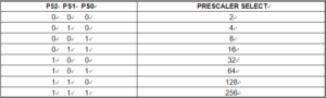
watchdog timer scheme
The time-out period is obtained using the following equation:
OSC
´ 214 ´PRESCALER ´ 1000 ´ 12 mS
Before Watchdog time-out occurs, the program must clear the 14-bit timer by writing 1 to WDTC.6 (CLRW). After 1 is written to this bit, the 14-bit timer, prescaler and this bit will be reset on the next instruction cycle. The Watchdog timer is cleared on reset.
Break WINBOND MCU W78E516 Eeprom Memory
When we try to Break WINBOND MCU W78E516 Eeprom Memory, there is an issue which is unable to avoid which is called EMI emission, and engineer need to figure out the way to reduce this Electro-magnetic emission interference. below we are going to introduce the cause of this interference and the way to reduce it:
Because of on-chip Flash EPROM, when a program is running in internal ROM space, the ALE will be unused. The transition of ALE will cause noise, so it can be turned off to reduce the EMI emission if it is useless. Turning off the ALE signal transition only requires setting the bit 0 of the AUXR SFR, which is located at 08Eh.
When ALE is turned off, it will be reactivated when the program accesses external ROM/RAM data or jumps to execute an external ROM code. The ALE signal will turn off again after it has been completely accessed or the program returns to internal ROM code space. The AO bit in the AUXR register, when set, disables the ALE output.
In order to reduce EMI emission from oscillation circuitry, W78E51B allows user to diminish the gain of on-chip oscillator amplifiers by using programmer to clear the B7 bit of security register. Once B7 is set to 0, a half of gain will be decreased after Break WINBOND MCU W78E516 Eeprom Memory.
Care must be taken if user attempts to diminish the gain of oscillator amplifier, reducing a half of gain may effect to external crystal operating improperly at high frequency above 24 MHz. The value of R and C1, C2 may need adjustment while running at lower gain before BREAK IC.
Crack Motorola MC68HC05B6 Microcontroller
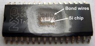
Crack Motorola MC68HC05B6 Microcontroller by focus ion beam to modify MCU circuitry pattern for the purpose of reset encryption status, then the firmware can be readout from MCU;
the Motorola MC68HC05B6 microcontroller has a Mask ROM bootloader which prevents user code upload if the security bit is set. The part of the code responsible for the security. It checks the contents of the first byte in the EEPROM and if the bit 0, assigned as a security fuse, is programmed then the CPU goes into endless loop.
That sort of protection could be relatively easy defeated. As the CPU performs only one instruction in the loop, all the attacker has to do is apply different clock glitches to cause CPU malfunction. He does not even have to carefully synchronise the attack to microcontroller’s CPU clock signal, as doing glitches at a random time will give a success in a short number of attempts. Glitches could be inserted relatively easy without the use of any external generators by short circuiting the crystal resonator for a short time.
When the resonator starts it produces oscillations at different harmonics which cause many glitches. In most cases the attack has to be applied at a certain clock cycle to cause the desired result. In this case it is better to use either a signal pattern generator which can supply all the necessary signals to the chip or built such a generator using an FPGA prototyping board.
 Tags:
Tags:
Restore Winbond Microcontroller W78E058 Heximal
We can Restore Winbond Microcontroller W78E058 Heximal, please view the Microcontroller W78E058 features for your reference:
FUNCTIONAL DESCRIPTION:
The W78E058 architecture consists of a core controller surrounded by various registers, five general purpose I/O ports, 128 bytes of RAM, two timer/counters, and a serial port. The processor supports 111 different opcodes and references both a 64K program address space and a 64K data storage space.
NEW DEFINED PERIPHERAL:
In order to be more suitable for I/O, an extra 4-bit bit-addressable port P4 and two external interrupt
INT2 , INT3 has been added to either the PLCC or QFP 44 pin package. And description follows:
INT2 / INT3
Two additional external interrupts, INT2 and INT3 , whose functions are similar to those of external interrupt 0 and 1 in the standard 80C52. The functions/status of these interrupts are determined/shown by the bits in the XICON (External Interrupt Control) register. The XICON register is bit-addressable but is not a standard register in the standard 80C52. Its address is at 0C0H. To set/clear bits in the XICON register, one can use the “SETB (/CLR) bit” instruction. For example, “SETB 0C2H” sets the EX2 bit of XICON when Restore Winbond Microcontroller W78E058 Heximal.
XICON – external interrupt control (C0H)
| PX3 | EX3 | IE3 | IT3 | PX2 | EX2 | IE2 | IT2 |
PX3: External interrupt 3 priority high if set EX3: External interrupt 3 enable if set
IE3: If IT3 = 1, IE3 is set/cleared automatically by hardware when interrupt is detected/serviced IT3: External interrupt 3 is falling-edge/low-level triggered when this bit is set/cleared by software PX2: External interrupt 2 priority high if set
EX2: External interrupt 2 enable if set
IE2: If IT2 = 1, IE2 is set/cleared automatically by hardware when interrupt is detected/serviced IT2: External interrupt 2 is falling-edge/low-level triggered when this bit is set/cleared by software after Restore Winbond Microcontroller W78E058 Heximal
Decode Winbond Chip W78E065 Internal Memory
We can Decode Winbond Chip W78E065 Internal Memory, please view the Winbond Chip W78E065 features for your reference:
The W78E065 is an 8-bit microcontroller which can accommodate a wider frequency range with low power consumption. The instruction set for the W78E065 is fully compatible with the standard 8051. The W78E065 contains an 4K bytes Flash EPROM; a 128 bytes RAM; four 8-bit bi-directional and bit- addressable I/O ports; an additional 4-bit I/O port P4; two 16-bit timer/counters; a hardware watchdog timer and a serial port.
These peripherals are supported by seven sources two-level interrupt capability. To facilitate programming and verification, the Flash EPROM inside the W78E51B allows the program memory to be programmed and read electronically. Once the code is confirmed, the user can protect the code for security when Decode Winbond Chip W78E065 Internal Memory.
The W78E065 microcontroller has two power reduction modes, idle mode and power-down mode, both of which are software selectable. The idle mode turns off the processor clock but allows for continued peripheral operation. The power-down mode stops the crystal oscillator for minimum power consumption. The external clock can be stopped at any time and in any state without affecting the processor after Decode Winbond Chip W78E065 Internal Memory.
2. FEATURES
Fully static design 8-bit CMOS microcontroller
Wide supply voltage of 4.5V to 5.5V
128 bytes of on-chip scratchpad RAM
4 KB On-chip Flash EPROM
64 KB program memory address space
64 KB data memory address space
Four 8-bit bi-directional ports
One extra 4-bit bit-addressable I/O port, additional INT2 / INT3
(available on 44-pin PLCC/QFP package)
Two 16-bit timer/counters
One full duplex serial port(UART)
Watchdog Timer
Seven sources, two-level interrupt capability
EMI reduction mode
Built-in power management
Code protection mechanism
Clock glitches, one of the most important way of IC attack
Clock-signal glitches are currently the simplest and most practical ones. In real application glitches are normally used to replace conditional jump instructions and test instructions preceding them. They create a window of vulnerability in the processing stages of many security cryptographic barriers by simply preventing the execution of the code that detects an unsuccessful authentication attempt. Instruction glitches can also be used to extend the runtime of loops, for example, in serial port output routines to see more of the memory after the output buffer, or to reduce the number of loops in cryptographic operation to transform the cipher into a weak one.
To perform a glitch, the clock frequency should be temporarily increased for one or more half cycles so that some flip-flops sample their input before the new state has reached them. As clock glitches are normally aimed at CPU instruction flow, they are not very effective for devices with hardware implementations of security protection. Therefore it is practical to use clock glitches only when attacking microcontrollers with software programming interfaces or some smartcards.
Break Atmel AVR MCU ATmega8535L Heximal
We can break atmel avr mcu ATMEGA8535L heximal, please view the atmel avr mcu ATMEGA8535L features for your reference:
The ATmega8535 provides all the features of the ATmega8535L. In addition, several new features are added. The ATmega8535 is backward compatible with ATmega8535L in most cases. However, some incompatibilities between the two atmel avr mcus exist.
To solve this problem, an ATmega8535L compatibility mode can be selected by programming the S8535C fuse. ATmega8535 is pin compatible with ATmega8535L, and can replace the AT90S8535 on current Printed Circuit Boards. However, the location of fuse bits and the electrical characteristics differs between the two devices.
Port A serves as the analog inputs to the A/D Converter. Port A also serves as an 8-bit bi-directional I/O port, if the A/D Converter is not used. Port pins can provide internal pull-up resistors (selected for each bit). The Port A output buffers have symmetrical drive characteristics with both high sink and source capability before break atmel avr mcu.
When pins PA0 to PA7 are used as inputs and are externally pulled low, they will source current if the internal pull-up resistors are activated.
The Port A pins are tri-stated when a reset condition becomes active, even if the clock is not running. Port B is an 8-bit bi-directional I/O port with internal pull-up resistors (selected for each bit). The Port B output buffers have symmetrical drive characteristics with both high sink and source capability after Break Atmel AVR MCU ATmega8535L Heximal.
As inputs, Port B pins that are externally pulled low will source current if the pull-up resistors are activated. The Port B pins are tri-stated when a reset condition becomes active, even if the clock is not running. Port C is an 8-bit bi-directional I/O port with internal pull-up resistors (selected for each bit). The Port C output buffers have symmetrical drive characteristics with both high sink and source capability.
As inputs, Port C pins that are externally pulled low will source current if the pull-up resistors are activated. The Port C pins are tri-stated when a reset condition becomes active, even if the clock is not running. Port D is an 8-bit bi-directional I/O port with internal pull-up resistors (selected for each bit). The Port D output buffers have symmetrical drive characteristics with both high sink and source capability when Break Atmel AVR MCU ATmega8535L Heximal.
As inputs, Port D pins that are externally pulled low will source current if the pull-up resistors are activated. The Port D pins are tri-stated when a reset condition becomes active, even if the clock is not running before break IC.