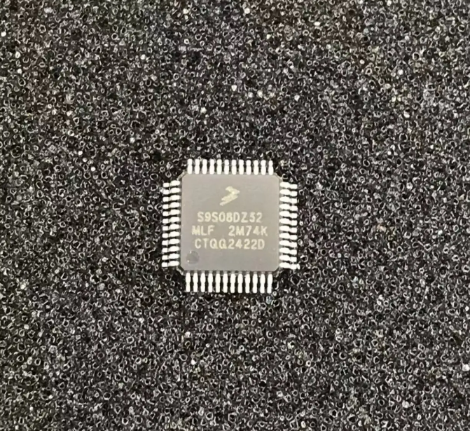
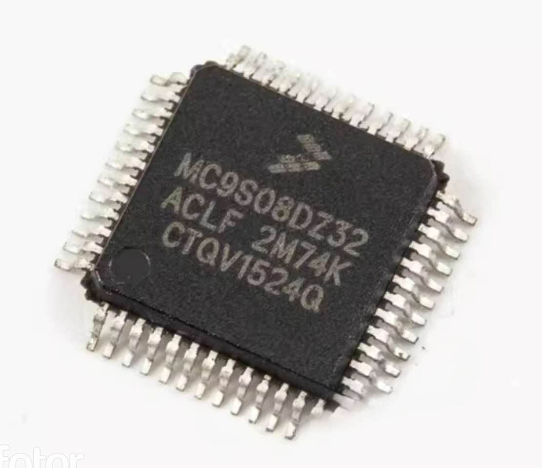
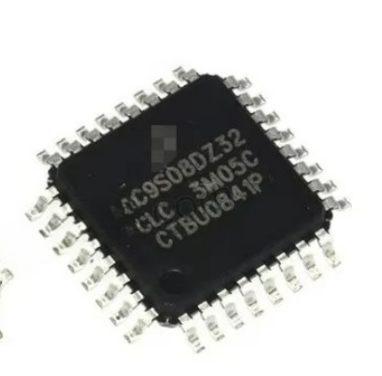
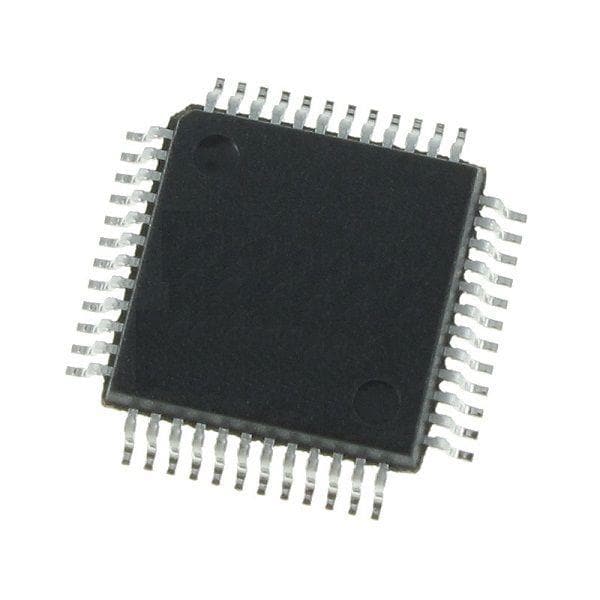
 Recover Chip MC9S08DZ32ACLC Firmware
The MC9S08DZ32ACLC microcontroller, developed by Freescale (now NXP), is widely used in automotive, industrial, and consumer electronics applications. Its popularity stems from its reliable performance, low power consumption, and robust integration of flash memory, EEPROM, and peripheral features. However, recovering firmware from this protected and embedded chip poses significant challenges due to its security mechanisms. At Circuit Engineering Co., Ltd, we offer professional and precise services to recover Chip MC9S08DZ32ACLC firmware, enabling access to valuable system-level data and binary files for legitimate engineering and recovery purposes.
Why Recover MC9S08DZ32ACLC Firmware?
This chip is commonly deployed in automotive control modules, dashboards, sensors, and smart motor applications. Engineers, OEMs, and repair technicians often face situations where the original firmware is lost, corrupted, or no longer accessible due to locked or encrypted flash memory. In such cases, recreating the product, cloning behavior, or simply restoring the embedded function becomes impossible without access to the original firmware. That’s where our service becomes essential.
Our Advanced Firmware Recovery Process
We utilize a combination of hardware probing, software cracking, and firmware decoding techniques to unlock, decrypt, and extract the firmware from the flash and EEPROM memory inside the MC9S08DZ32ACLC. Our expertise allows us to crack secured chips and duplicate the binary/heximal files while maintaining data integrity and completeness.
Once access is established, we copy and clone the program data, restoring it into a readable hex file or reconstructing it into assembly or source code formats as needed. This allows our clients to not only recover the program but also analyze, test, or modify it for updated product development, security audits, or system migration.
Key Services We Provide:
- Recover Chip MC9S08DZ32ACLC Firmware from locked or secured systems
- Clone and duplicate the embedded flash contents into new units
- Restore lost firmware files, EEPROM data, or archived program structures
- Decode and decrypt binary firmware for analysis or reuse
- Unlock encrypted program memory for reverse engineering or debugging
- Provide reconstructed heximal or binary files for reprogramming or documentation
Unique Features of the MC9S08DZ32ACLC
This 8-bit MCU from Freescale features:
- Up to 32KB of flash memory and 2KB EEPROM
- Internal clock generators and multiple communication interfaces (CAN, SCI, SPI, I²C)
- Enhanced control and diagnostics support for automotive-grade environments
- Advanced interrupt handling and low EMI design, making it ideal for mission-critical applications
Its robust security options—including memory protection schemes—make firmware access nearly impossible without specialized equipment and technical insight. That’s why your choice of service provider is critical.
Trusted, Confidential, and Accurate
All projects handled by our engineering team are executed with strict confidentiality and technical accuracy. Whether you’re looking to restore a malfunctioning device, duplicate firmware for production, or analyze a secured program archive, we deliver results efficiently and securely.
We can Recover Chip MC9S08DZ32ACLC Firmware, please view below the Chip MC9S08DZ32ACLC features for your reference:
8-Bit HCS08 Central Processor Unit (CPU)
· 40-MHz HCS08 CPU (20-MHz bus)
· HC08 instruction set with added BGND instruction
· Support for up to 32 interrupt/reset sources
On-Chip Memory
· Flash read/program/erase over full operating voltage and temperature
— MC9S08DZ60 = 60K
— MC9S08DZ48 = 48K
— MC9S08DZ32 = 32K
— MC9S08DZ16 = 16K
· Up to 2K EEPROM in-circuit programmable memory;
8-byte single-page or 4-byte dual-page erase sector;
Program and Erase while executing Flash; Erase abort
· Up to 4K random-access memory (RAM)
Power-Saving Modes
· Two very low power stop modes
· Reduced power wait mode
· Very low power real time interrupt for use in run, wait, and stop Clock Source Options
· Oscillator (XOSC) — Loop-control Pierce oscillator;
Crystal or ceramic resonator range of 31.25 kHz to 38.4 kHz or 1 MHz to 16 MHz
· Multi-purpose Clock Generator (MCG) — PLL and FLL modes (FLL capable of 1.5% deviation using internal temperature compensation); Internal reference clock with trim adjustment (trimmed at factory, with trim value stored in flash); External reference with oscillator/resonator options in the process of Copy microcontroller
System Protection
· Watchdog computer operating properly (COP) reset with option to run from backup dedicated 1-kHz internal clock source or bus clock
· Low-voltage detection with reset or interrupt; selectable trip points
· Illegal opcode detection with reset
· Illegal address detection with reset
· Flash block protect
· Loss-of-lock protection
Peripherals
· ADC — 24-channel, 12-bit resolution, 2.5 ìs conversion time, automatic compare function, temperature sensor, internal bandgap reference channel
· ACMPx — Two analog comparators with selectable interrupt on rising, falling, or either edge of comparator output; compare option to fixed internal bandgap reference voltage.
· MSCAN — CAN protocol – Version 2.0 A, B; standard and extended data frames; Support for remote frames; Five receive buffers with FIFO storage scheme; Flexible identifier acceptance filters programmable as: 2 x 32-bit, 4 x 16-bit, or 8 x 8-bit
· SCIx — Two SCIs supporting LIN 2.0 Protocol and SAE J2602 protocols; Full duplex non-return to zero (NRZ); Master extended break generation; Slave extended break detection; Wakeup on active edge.
· SPI — Full-duplex or single-wire bidirectional; Double-buffered transmit and receive; Master or Slave mode; MSB-first or LSB-first shifting
· IIC — Up to 100 kbps with maximum bus loading; Multi-master operation; Programmable slave address; General Call Address; Interrupt driven byte-by-byte data transfer
· TPMx — One 6-channel (TPM1) and one 2-channel (TPM2); Selectable input capture, output compare, or buffered edge-aligned PWM on each channel.
· RTC — (Real-time counter) 8-bit modulus counter with binary or decimal based prescaler; Real-time clock capabilities using external crystal and RTC for precise time base, time-of-day, calendar or task scheduling functions; Free running on-chip low power oscillator (1 kHz) for cyclic wake-up without external components Input/Output
· 53 general-purpose input/output (I/O) pins and 1 input-only pin
· 24 interrupt pins with selectable polarity on each pin.
· Hysteresis and configurable pull device on all input pins.
· Configurable slew rate and drive strength on all output pins.
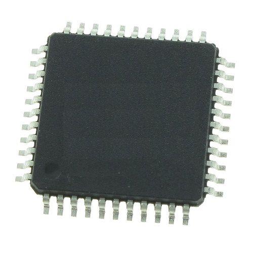
Package Options
· 64-pin low-profile quad flat-pack (LQFP) — 10×10 mm
· 48-pin low-profile quad flat-pack (LQFP) — 7×7 mm
· 32-pin low-profile quad flat-pack (LQFP) — 7×7 mm
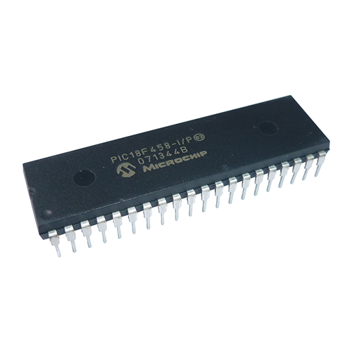
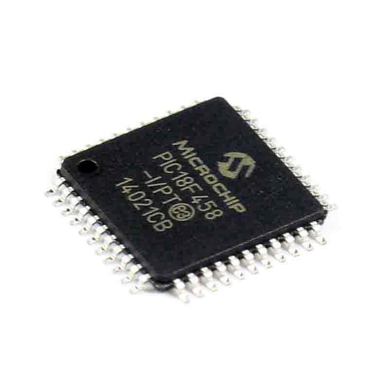
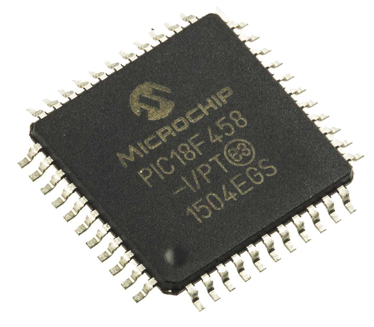
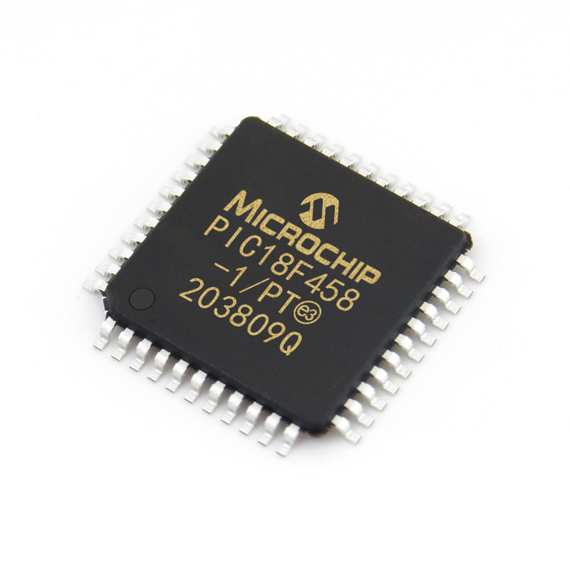
Copy IC PIC18F458 Binary
The Microchip PIC18F458 is a high-performance 8-bit microcontroller widely used in automotive, industrial automation, and communication systems. With its integrated CAN module, flexible memory architecture, and rich peripheral features, this chip is a cornerstone of many embedded applications. However, when the original firmware is protected, encrypted, or locked, users may find it nearly impossible to access, replicate, or modify the system behavior. That’s where our advanced service to Copy IC PIC18F458 Binary comes in.
Why Recovering PIC18F458 Binary Matters
Whether you’ve lost the original development source, need to restore legacy systems, or want to duplicate an existing board for spare parts or upgrade, recovering the binary, heximal, or flash memory from a secured PIC18F458 is critical. This chip often contains proprietary logic in its EEPROM, data memory, and program flash, making any reverse engineering task extremely sensitive and technical.
Unfortunately, Microchip implements hardware-level security mechanisms in the PIC18 series, including code protection fuses and readback restrictions. These are designed to prevent unauthorized access—but they also pose significant barriers to engineers who need to access their own systems due to misplaced source files or failed developers.
Our Expertise: Crack, Decode, and Recover
Our professional team specializes in cracking, decoding, and decrypting protected microcontrollers like the PIC18F458. We employ cutting-edge tools and proven methodologies to unlock, open, and copy both the firmware and binary archives from secured devices. Once extracted, we provide clients with clean, reusable HEX files, and when required, assist in converting them into source code or documentation for further development.
Here’s how we can help:
- Binary Extraction from protected PIC18F458 microcontrollers
- Cloning & Duplicating fully functional firmware for spare or replacement boards
- Decrypting and Dumping Flash/EEPROM memory contents
- Rebuilding Heximal and Source Files from compiled program memory
- Analyzing and Modifying recovered firmware for upgrades or security testing
All operations are conducted with strict confidentiality, ensuring the protection of intellectual property and compliance with relevant legal and ethical standards.
Features of the PIC18F458 That Make It Unique
The PIC18F458 features:
- 32KB of Flash Program Memory
- CAN (Controller Area Network) interface
- 1.5KB SRAM and 256 Bytes EEPROM
- 10-bit ADC, Timers, CCP modules, and Enhanced USART
- In-Circuit Serial Programming (ICSP) and Debug support
These make it an excellent controller for data-driven embedded systems. However, its robustness also adds complexity when attempting to recover data from a protected or encrypted device.
Applications We Support
The PIC18F458 is commonly found in:
- Automotive ECU and dashboard systems
- Industrial sensors and automation controllers
- Network communication devices with CAN bus
- Consumer electronics with real-time control needs
Our services are tailored for hardware developers, repair technicians, embedded engineers, and system integrators who depend on accurate and reliable firmware duplication or data recovery for ongoing support, migration, or development.
Whether you’ve lost access to the original source, or simply need to copy IC PIC18F458 binary from a secured system for legitimate purposes, our team is equipped to help. Contact us today to discuss how we can clone, unlock, and recover your valuable embedded programs quickly and securely.
Copy IC PIC18F458 Binary from its locked memory include flash and eeprom, the firmware will be same as original Microcontroller PIC18F458 program and can be replicated to other blank MCU;
Power-Managed Modes:
Peripheral Highlights:
Run: CPU on, Peripherals on
Idle: CPU off, Peripherals on
Sleep: CPU off, Peripherals off
Idle mode Currents Down to 6.1 ìA Typical
Sleep mode Current Down to 0.2 ìA Typical
Timer1 Oscillator: 1 ìA, 32 kHz, 2V
Watchdog Timer: 1.7 ìA
Two-Speed Oscillator Start-up
High-Current Sink/Source 25 mA/25 mA
Three External Interrupts
One Capture/Compare/PWM (CCP) module
Enhanced Capture/Compare/PWM (ECCP) module
(40/44-pin devices only):
– One, two or four PWM outputs
– Selectable polarity
– Programmable dead time
Flexible Oscillator Structure:
· Four Crystal modes, up to 40 MHz
· 4x Phase Lock Loop (PLL) – Available for Crystal and Internal Oscillators)
· Two External RC modes, up to 4 MHz
· Two External Clock modes, up to 40 MHz
· Internal Oscillator Block:
– Fast wake from Sleep and Idle, 1 ìs typical
– 8 user-selectable frequencies, from 31 kHz to 8 MHz
– Provides a complete range of clock speeds, from 31 kHz to 32 MHz when used with PLL
– User-tunable to compensate for frequency drift
· Secondary Oscillator using Timer1 @ 32 kHz
· Fail-Safe Clock Monitor
– Auto-shutdown and auto-restart which can be applied for crack MCU memory
Master Synchronous Serial Port (MSSP) module
Supporting 3-Wire SPI (all 4 modes) and I2C™
Master and Slave modes
Enhanced Addressable USART module
– Supports RS-485, RS-232 and LIN/J2602
– RS-232 operation using internal oscillator block
– Auto-wake-up on Start bit
– Auto-Baud Detect
10-Bit, up to 11-Channel Analog-to-Digital Converter (A/D) module, up to 100 ksps
– Auto-acquisition capability
– Conversion available during Sleep
Dual Analog Comparators with Input Multiplexing
– Allows for safe shutdown if peripheral clock stops
Special Microcontroller Features:
· C Compiler Optimized Architecture with Optional Extended Instruction Set
· 100,000 Erase/Write Cycle Enhanced Flash Program Memory Typical
· 1,000,000 Erase/Write Cycle Data EEPROM Memory Typical
· Flash/Data EEPROM Retention: > 40 Years
· Self-Programmable under Software Control
· Priority Levels for Interrupts
· 8 x 8 Single-Cycle Hardware Multiplier
· Extended Watchdog Timer (WDT):
– Programmable period from 41 ms to 131s
· Single-Supply 5V In-Circuit Serial Programming™ (ICSP™) via Two Pins
· In-Circuit Debug (ICD) via Two Pins
· Wide Operating Voltage Range: 2.0V to 5.5V ECAN Technology Module Features:
· Message Bit Rates up to 1 Mbps
· Conforms to CAN 2.0B Active Specification
· Fully Backward Compatible with PIC18XXX8 CAN modules
· Three Modes of Operation:
– Legacy, Enhanced Legacy, FIFO
· Three Dedicated Transmit Buffers with Prioritization
· Two Dedicated Receive Buffers
· Six Programmable Receive/Transmit Buffers
· Three Full 29-Bit Acceptance Masks
· 16 Full 29-Bit Acceptance Filters w/Dynamic Association
· DeviceNet™ Data Byte Filter Support
· Automatic Remote Frame Handling
· Advanced Error Management Features
Attack Chip PIC18F66K90 software
Attack Chip PIC18F66K90 software
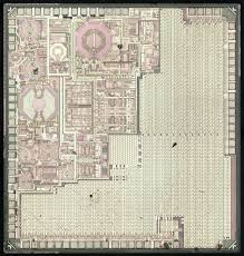
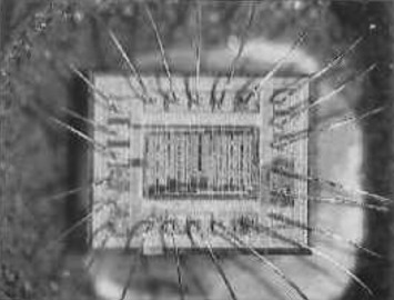
Attack Chip PIC18F66K90 starts from decapsulate the microcontroller silicon package and locate the security fuse bit which has been viewed an most commonly way to crack MCU, then extract the software out from the memory;
Low-Power Features:
· Power-Managed modes:
– Run: CPU on, peripherals on
– Idle: CPU off, peripherals on
– Sleep: CPU off, peripherals off
· Two-Speed Oscillator Start-up
· Fail-Safe Clock Monitor
· Power-Saving Peripheral Module Disable (PMD)
· Ultra Low-Power Wake-up
· Fast Wake-up, 2 ms Typical
· Low-Power WDT, 300 nA Typical
· Ultra Low 50 nA Input Leakage
· Run mode Currents Down to very low 5.5 mA, Typical
· Idle mode Currents Down to very low 2.2 mA, Typical
· Sleep mode Current Down to very low 20 nA, Typical
· RTCC Current Down to very low 700 nA, Typical
· LCD Current Down to very low 300 nA, Typical
LCD Driver and Keypad Features:
· Direct LCD Panel Drive Capability:
– Can drive LCD panel while in Sleep mode
· Up to 48 Segments and 192 Pixels, Software-Selectable
· Programmable LCD Timing module:
– Multiple LCD timing sources available
– Up to four commons: static, 1/2, 1/3 or 1/4 multiplex
– Bias configuration: Static, 1/2 or 1/3
· Low-Power Resistor Bias Network for LCD
Peripheral Highlights:
· Ten or eight CCP/ECCP modules:
– Seven Capture/Compare/PWM (CCP) modules
– Three Enhanced Capture/Compare/PWM (ECCP) modules
· Eleven 8/16-Bit Timer/Counter modules:
– Timer0 – 8/16-bit timer/counter with 8-bit programmable prescaler
– Timer1,3,5,7 – 16-bit timer/counter
– Timer2,4,6,8,10,12 – 8-bit timer/counter
· Three Analog Comparators
· Configurable Reference Clock Output
· Hardware Real-Time Clock and Calendar (RTCC) module with Clock, Calendar and Alarm Functions
– Time-out from 0.5s to 1 year
· Charge Time Measurement Unit (CTMU)
– Capacitance measurement for mTouch™ Sensing
– Time measurement with 1 ns typical resolution
· High-Current Sink/Source 25 mA/25 mA (PORTB and PORTC)
· Up to Four External Interrupts
· Two Master Synchronous Serial Port (MSSP) modules:
– 3/4-wire SPI (supports all four SPI modes)
– I2C™ Master and Slave mode
Special Microcontroller Features:
· Priority Levels for Interrupts
Operating Voltage Range: 1.8V to 5.5V
On-Chip 3.3V Regulator
Operating Speed up to 64 MHz
Up to 128 Kbytes On-Chip Flash Program Memory Data EEPROM of 1,024 Bytes
4K x 8 General Purpose Registers (SRAM)
10,000 Erase/Write Cycle Flash Program
Memory, Typical 1,000,000 Erase/write Cycle Data EEPROM
Memory, Typical Flash Retention 40 Years, Minimum
Three Internal Oscillators: LF-INTRC (31 kHz),
MF-INTOSC (500 kHz) and HF-INTOSC (16 MHz)
Self-Programmable under Software Control
· 8 x 8 Single-Cycle Hardware Multiplier
· Extended Watchdog Timer (WDT):
– Programmable period from 4 ms to 4,194s (about 70 minutes)
· In-Circuit Serial Programming™ (ICSP™) via
Two Pins
· In-Circuit Debug via Two Pins
· Programmable:
– BOR
– LVD
· Two Enhanced Addressable USART modules:
– LIN/J2602 support
– Auto-Baud Detect (ABD)
· 12-Bit A/D Converter with up to 24 Channels:
– Auto-acquisition and Sleep operation
– Differential Input mode of operation
Attack Microcontroller PIC18F66K90 Heximal
Attack Microcontroller PIC18F66K90 Heximal
Attack Microcontroller PIC18F66K90 locked memory cell include flash and eeprom, disable the security fuse bits and get access to the databus of MCU then readout the Heximal and clone content to new IC;
Low-Power Features:
· Power-Managed modes:
– Run: CPU on, peripherals on
– Idle: CPU off, peripherals on
– Sleep: CPU off, peripherals off
· Two-Speed Oscillator Start-up
· Fail-Safe Clock Monitor
· Power-Saving Peripheral Module Disable (PMD)
· Ultra Low-Power Wake-up
· Fast Wake-up, 2 ms Typical
· Low-Power WDT, 300 nA Typical
· Ultra Low 50 nA Input Leakage
· Run mode Currents Down to very low 5.5 mA, Typical
· Idle mode Currents Down to very low 2.2 mA, Typical
· Sleep mode Current Down to very low 20 nA, Typical
· RTCC Current Down to very low 700 nA, Typical
· LCD Current Down to very low 300 nA, Typical LCD Driver and Keypad Features:
· Direct LCD Panel Drive Capability:
– Can drive LCD panel while in Sleep mode
· Up to 48 Segments and 192 Pixels, Software-Selectable
· Programmable LCD Timing module:
– Multiple LCD timing sources available
– Up to four commons: static, 1/2, 1/3 or 1/4 multiplex
– Bias configuration: Static, 1/2 or 1/3
· Low-Power Resistor Bias Network for LCD Peripheral Highlights:
· Ten or eight CCP/ECCP modules:
– Seven Capture/Compare/PWM (CCP) modules
– Three Enhanced Capture/Compare/PWM (ECCP) modules
· Eleven 8/16-Bit Timer/Counter modules:
– Timer0 – 8/16-bit timer/counter with 8-bit programmable prescaler
– Timer1,3,5,7 – 16-bit timer/counter
– Timer2,4,6,8,10,12 – 8-bit timer/counter
· Three Analog Comparators
· Configurable Reference Clock Output
· Hardware Real-Time Clock and Calendar (RTCC) module with Clock, Calendar and Alarm Functions
– Time-out from 0.5s to 1 year
· Charge Time Measurement Unit (CTMU):
– Capacitance measurement for mTouch™ Sensing
– Time measurement with 1 ns typical resolution
· High-Current Sink/Source 25 mA/25 mA (PORTB and PORTC)
· Up to Four External Interrupts
· Two Master Synchronous Serial Port (MSSP) modules:
– 3/4-wire SPI (supports all four SPI modes)
– I2C™ Master and Slave mode
Special Microcontroller Features:
· Priority Levels for Interrupts
Operating Voltage Range: 1.8V to 5.5V
On-Chip 3.3V Regulator
Operating Speed up to 64 MHz
Up to 128 Kbytes On-Chip Flash Program Memory Data EEPROM of 1,024 Bytes
4K x 8 General Purpose Registers (SRAM)
10,000 Erase/Write Cycle Flash Program
Memory, Typical 1,000,000 Erase/write Cycle Data EEPROM
Memory, Typical Flash Retention 40 Years, Minimum
Three Internal Oscillators: LF-INTRC (31 kHz),
MF-INTOSC (500 kHz) and HF-INTOSC (16 MHz)
Self-Programmable under Software Control
· 8 x 8 Single-Cycle Hardware Multiplier
· Extended Watchdog Timer (WDT):
– Programmable period from 4 ms to 4,194s (about 70 minutes)
· In-Circuit Serial Programming™ (ICSP™) via Two Pins
· In-Circuit Debug via Two Pins
· Programmable:
– BOR
– LVD
· Two Enhanced Addressable USART modules:
– LIN/J2602 support
– Auto-Baud Detect (ABD)
· 12-Bit A/D Converter with up to 24 Channels:
– Auto-acquisition and Sleep operation
– Differential Input mode of operation
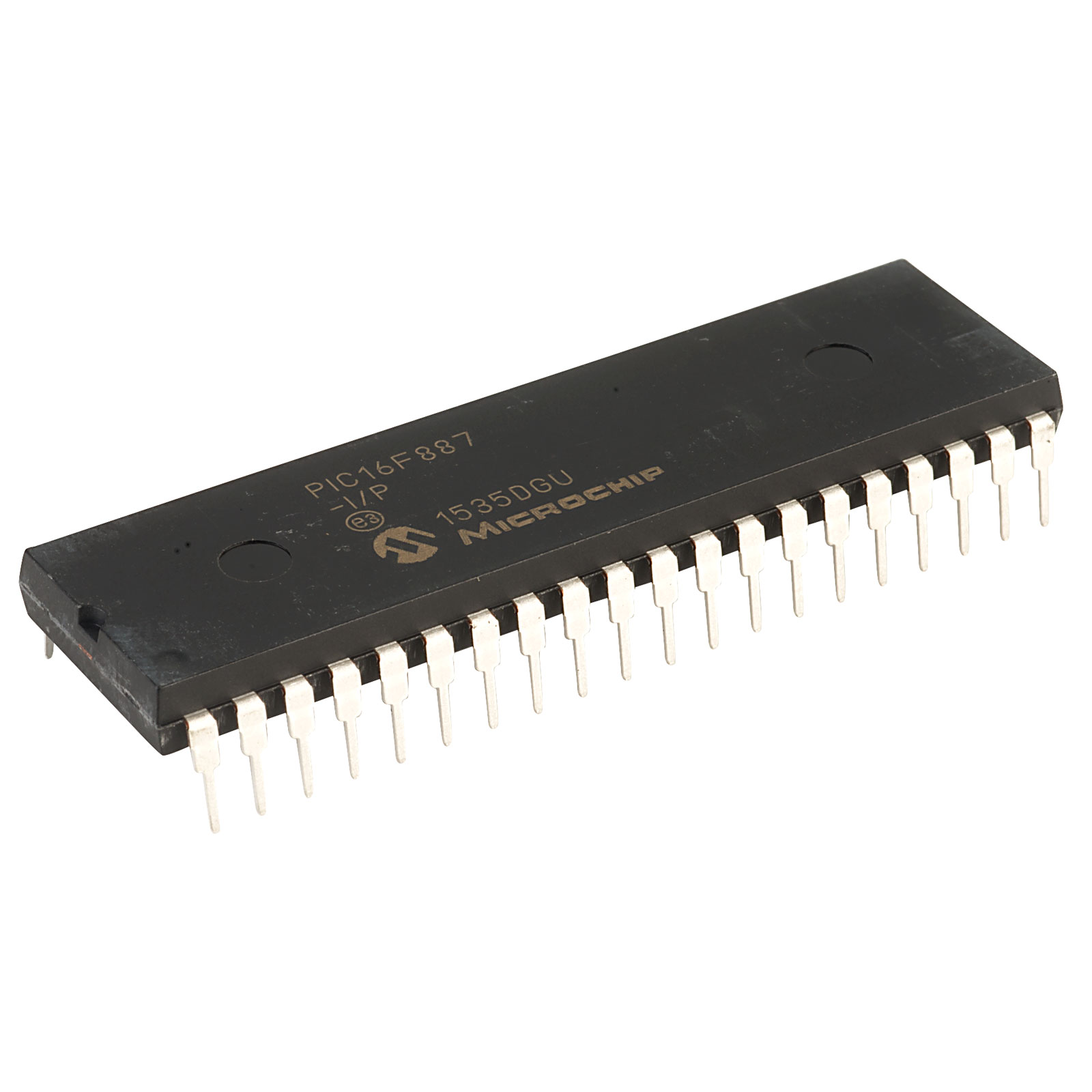
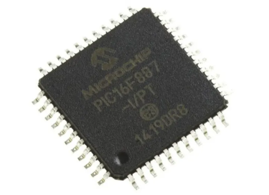
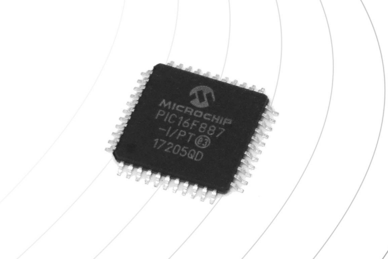
Attack MCU PIC16F887 Program
The Microchip PIC16F887 microcontroller is widely used in embedded systems for industrial, automotive, and consumer applications. Known for its versatility, low power consumption, and built-in peripherals, this 8-bit MCU features flash memory, EEPROM, and an internal oscillator, making it a popular choice for compact and cost-effective designs. However, its widespread use in protected and secured systems also means that its internal program and data are often locked or encrypted to prevent tampering or duplication.
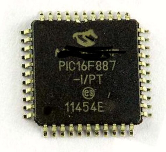
At circuit engineering co.,ltd, we offer advanced services to attack MCU PIC16F887 program protections and help clients restore, crack, or copy the original heximal firmware and binary contents. Whether you’ve lost the original source, need to clone a locked device, or require a duplicate for maintenance or migration, our reverse engineering solutions provide access to the flash, EEPROM, and program memory of secured PIC16F887 microcontrollers.
Attack MCU PIC16F887 tamper resistance system and readout the Program and data from its flash memory and eeprom memory, clone firmware to new IC which will provide the same functions as original Microcontroller PIC16F887;
Module: Analog-To-Digital Converter (ADC) Module
Selecting the VP6 reference as the analog input source (CHS<3:0> = 1111) for the ADC conversion after sampling another analog channel with input voltages approximately greater than 3.6V can temporarily disturb the HFINTOSC oscillator.
4. Module: MSSP (SPI Master Mode)
With MSSP in SPI Master mode, FOSC/64 or Timer2/2 clock rate and CKE = 0, a write collision may occur if SSPBUF is loaded immediately after the transfer is complete after Attack MCU. A delay may be required after the MSSP Interrupt Flag bit, SSPIF, is set or the Buffer Full bit, BF, is set and before writing SSPBUF. If the delay is insufficiently short, a write register and NOT during the start of an actual ADC conversion using the GO/DONE bit in the ADCON0 register.
Microchip has integrated multiple protection mechanisms into the PIC16F887 to prevent unauthorized access. From code protection bits to memory locking, these security features are designed to make decrypting or decoding the firmware difficult for the average user. However, with years of hands-on experience and access to proprietary techniques and tools, our engineering team can hack these barriers and retrieve the original data, even from obfuscated or heavily encrypted firmware images.
We don’t simply dump raw memory—we provide complete, structured hex files or even human-readable source code where possible. Our process may involve full-chip readout, flash memory analysis, EEPROM data extraction, and program reconstruction, ensuring nothing critical is left behind.
This only occurs when selecting the VP6 reference ADC channel using the CHS<3:0> bits in the ADCON0 collision may occur as indicated by the WCOL bit being set.
Select an ADC channel with input voltages lower than 3.6V prior to selecting the VP6 reference voltage input. Any analog channel can be used, even if that channel is configured as a digital I/O (configured as an output) that is driving the output pin low when Attack MCU. An alternative is to configure the CVREF module to output a voltage less than 3.6V and then selecting that analog channel CHS<3:0> = 1110 as the analog input source.
Add a software delay of one SCK period after detecting the completed transfer and prior to updating the SSPBUF contents. Verify the WCOL bit is clear after writing SSPBUF. If the WCOL is set, clear the bit in software and rewrite the SSPBUF register.
Date Codes that pertain to this issue:
All engineering and production devices.
Affected Silicon Revisions
The PIC16F887 is widely appreciated for:
- 14-bit instruction set with 368 bytes of RAM and 256 bytes of EEPROM
- 8K x 14 words of Flash program memory
- 35 flexible I/O pins and support for multiple communication protocols (USART, SPI, I2C)
- Integrated ADCs, comparators, and timers
- Low power sleep modes for energy-sensitive applications
This embedded chip is commonly found in:
- Industrial sensor systems
- Smart home controllers
- HVAC controllers
- Educational development boards
- Low-cost automation devices
Due to its versatility, it’s often reused across multiple projects—making it especially frustrating when firmware is locked or when original source code is lost.
Our clients come from diverse industries—repair technicians, industrial OEMs, system integrators, and even researchers. We offer personalized consultation and confidential service to ensure that your objectives are met, whether you need to open a firmware file, clone a working board, or duplicate a system before a hardware refresh.
Our full service includes:
- Decryption and decoding of protected PIC16F887 firmware
- Memory dump and recovery of hex/binary files
- Reverse engineering of flash and EEPROM contents
- Optional conversion to partial or full C-like source code
If you need to attack MCU PIC16F887 program security for legitimate repair, recovery, or development purposes, our service delivers reliable, efficient, and professional support. We understand the complexity of protected embedded systems and are ready to help you regain control of your devices by unlocking valuable program archives and firmware data.
Contact Circuit Engineering CO., LTD today to learn more or schedule a consultation.
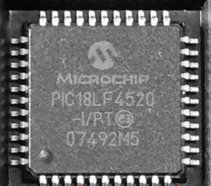
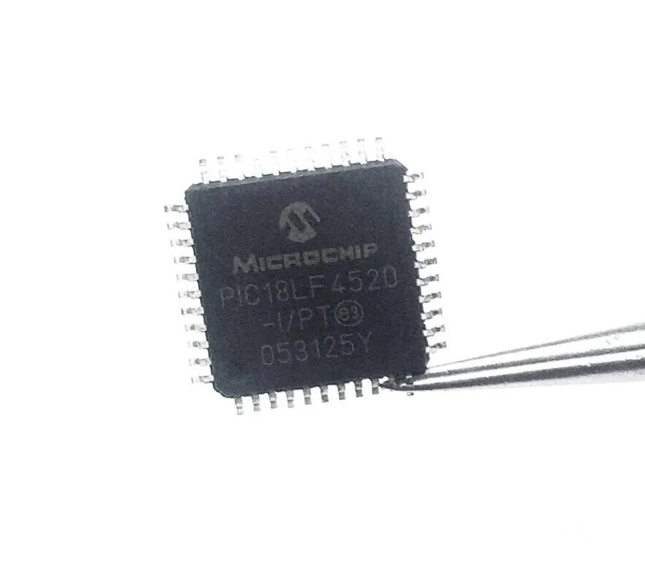
Attack IC PIC18LF4520 Program
The MICROCHIP PIC18LF4520 is a powerful 8-bit microcontroller widely used in industrial, automotive, and consumer electronics applications. Known for its rich peripheral set, low power consumption, and high-performance features, this embedded chip is commonly implemented in critical systems requiring reliable and long-lasting control logic. However, when firmware becomes protected, encrypted, or locked, recovering the underlying program, binary, or source code can be a daunting task—especially for system integrators, engineers, or developers dealing with legacy systems, code loss, or product redesign.
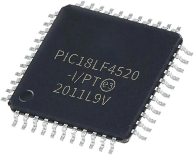
At Circuit Engineering CO., LTD, we specialize in professional services to attack IC PIC18LF4520 program and help clients restore, crack, hack, or decrypt the hidden firmware from the chip’s internal memory. Whether it is the main flash, EEPROM, or data archive, our expert techniques allow us to safely open, unlock, and retrieve the essential heximal file needed for modification, backup, or duplication.
Attack IC PIC18LF4520 protective memory, cut off the security fuse of the memory and extract Program and data from the flash and eeprom, Clone the content to other new Microcontroller PIC18LF4520 for the same functions;
Power Management Features:
Peripheral Highlights (Continued):
Run: CPU on, Peripherals on
Idle: CPU off, Peripherals on
Sleep: CPU off, Peripherals off
Ultra Low 50nA Input Leakage
Run mode Currents Down to 11 ìA Typical
Idle mode Currents Down to 2.5 ìA Typical
Sleep mode Current Down to 100 nA Typical
Timer1 Oscillator: 900 nA, 32 kHz, 2V
Watchdog Timer: 1.4 ìA, 2V Typical
Two-Speed Oscillator Start-up
Unlike basic read-out attempts, our approach to attacking the PIC18LF4520 program involves a combination of low-level hardware analysis, voltage glitching, and advanced microprobing when necessary. These techniques are designed to bypass the chip’s security fuses and read-protection mechanisms that usually prevent access to secured firmware. Once the heximal binary is extracted, we can decode and disassemble it, converting the firmware into readable formats for debugging or porting.
We understand that many clients may have lost their only copy of a program or inherited a product without source code access. That’s why we provide tailored solutions that go beyond basic data retrieval. Our services are designed to help:
- Recover lost firmware from damaged or legacy devices.
- Clone or duplicate a protected controller for scaling or prototyping.
- Reverse-engineer encrypted binaries to re-develop systems when documentation is missing.
- Unlock access to EEPROM data that may contain important system calibration or runtime parameters.
· Master Synchronous Serial Port (MSSP) module
Supporting 3-Wire SPI (all 4 modes) and I2C™ Master and Slave modes
· Enhanced Addressable USART module:
– Supports RS-485, RS-232 and LIN/J2602
– RS-232 operation using internal oscillator
block (no external crystal required)
– Auto-wake-up on Start bit
– Auto-Baud Detect
· 10-Bit, up to 13-Channel Analog-to-Digital (A/D)
Flexible Oscillator Structure:
· Four Crystal modes, up to 40 MHz
· 4x Phase Lock Loop (PLL) – Available for Crystal and Internal Oscillators
· Two External RC modes, up to 4 MHz
· Two External Clock modes, up to 40 MHz
· Internal Oscillator Block:
– Fast wake from Sleep and Idle, 1 ìs typical
– 8 use-selectable frequencies, from 31 kHz to 8 MHz
– Provides a complete range of clock speeds from 31 kHz to 32 MHz when used with PLL
– User-tunable to compensate for frequency drift
· Secondary Oscillator using Timer1 @ 32 kHz
· Fail-Safe Clock Monitor:
– Allows for safe shutdown if peripheral clock stops
Peripheral Highlights:
Converter module:
– Auto-acquisition capability
– Conversion available during Sleep
· Dual Analog Comparators with Input Multiplexing
· Programmable 16-Level High/Low-Voltage Detection (HLVD) module:
– Supports interrupt on High/Low-Voltage Detection
Special Microcontroller Features:
· C Compiler Optimized Architecture:
– Optional extended instruction set designed to optimize re-entrant code
· 100,000 Erase/Write Cycle Enhanced Flash
Program Memory Typical
· 1,000,000 Erase/Write Cycle Data EEPROM
Memory Typical
· Flash/Data EEPROM Retention: 100 Years Typical
· Self-Programmable under Software Control
High-Current Sink/Source 25 mA/25 mA
Three Programmable External Interrupts
Four Input Change Interrupts
Up to 2 Capture/Compare/PWM (CCP) modules,
· Priority Levels for Interrupts
· 8 x 8 Single-Cycle Hardware Multiplier
· Extended Watchdog Timer (WDT):
– Programmable period from 4 ms to 131s one with Auto-Shutdown (28-pin devices)
· Enhanced Capture/Compare/PWM (ECCP) module (40/44-pin devices only):
– One, two or four PWM outputs
– Selectable polarity
– Programmable dead time
– Auto-shutdown and auto-restart
· Single-Supply 5V In-Circuit Serial
Programming™ (ICSP™) via Two Pins
· In-Circuit Debug (ICD) via Two Pins
· Wide Operating Voltage Range: 2.0V to 5.5V
· Programmable Brown-out Reset (BOR) with Software Enable Option
The PIC18LF4520 stands out with features like nanoWatt technology, 10-bit ADC, 32 KB program memory, and dual USARTs—making it suitable for low-power and battery-powered applications. It is often deployed in secured embedded systems such as medical devices, motor controllers, industrial sensors, and power monitoring units. When these systems become inaccessible due to locked or encrypted firmware, downtime or redevelopment costs can escalate quickly.
That’s where our expertise provides immense value. Our ability to crack and extract locked firmware files from the PIC18LF4520 saves time, preserves original design intent, and allows for safe system replication or migration. We treat every engagement with the highest level of confidentiality. Our firmware attack and recovery services are designed for legitimate owners, OEMs, and system maintainers who need access to critical firmware for lawful purposes such as repair, maintenance, or migration. We do not support or condone unauthorized duplication of intellectual property.
If you need help attacking the IC PIC18LF4520 program, whether to decrypt firmware, duplicate a chip, or retrieve locked data, our expert team is ready to assist. Let us help you restore control over your embedded systems and provide solutions to move your project forward.
Break Chip SAF-C164CI-8EM Firmware
The Infineon SAF-C164CI-8EM is a powerful 16-bit microcontroller built for performance-critical embedded applications, commonly used in automotive, industrial control systems, and communication devices. Engineered with advanced peripheral integration and real-time processing capabilities, this chip is trusted in environments where reliability and timing are paramount.

However, the same strengths that make it suitable for mission-critical tasks—such as its protected memory structure, secured flash, and locked EEPROM regions—can pose major challenges when users need to break chip SAF-C164CI-8EM firmware to retrieve or modify system data. This is especially true in scenarios involving legacy systems, product redesigns, firmware migration, or unauthorized lockouts.
At Circuit ENGINEERING CO.,LTD, we specialize in unlocking, copying, and decoding complex, encrypted microcontroller firmware, including that of the SAF-C164CI-8EM. Our advanced techniques allow clients to recover the heximal, binary, or source code representations of a device’s flash, EEPROM, or embedded memory regions—even if these areas are locked, cracked, or obfuscated by protective logic.
The Infineon SAF-C164CI-8EM is part of the C164 microcontroller family and features:
- A 16-bit CPU core with up to 20 MHz operating frequency
- On-chip Flash memory and EEPROM
- Multiple timers, serial interfaces, and A/D converters
- Robust interrupt management for real-time responsiveness
Its combination of computational power and peripheral flexibility makes it suitable for automotive ECUs, process automation, industrial PLCs, and telecom modules.

Unfortunately, this level of integration often means the firmware is secured, leaving engineers unable to access the firmware file, or binary data needed for analysis, updates, or duplication.
Break Chip SAF-C164CI-8EM encrypted memory and extract the Firmware out from its flash and eeprom memory, then copy the program and data to blank Microcontroller cloning;
16-Bit Single-Chip Microcontroller C164CI/SI, C164CL/SL
· High Performance 16-bit CPU with 4-Stage Pipeline
– 80 ns Instruction Cycle Time at 25 MHz CPU Clock
– 400 ns Multiplication (16 × 16 bit), 800 ns Division (32 / 16 bit)
– Enhanced Boolean Bit Manipulation Facilities
– Additional Instructions to Support HLL and Operating Systems
– Register-Based Design with Multiple Variable Register Banks
– Single-Cycle Context Switching Support
– 16 MBytes Total Linear Address Space for Code and Data
– 1024 Bytes On-Chip Special Function Register Area
· 16-Priority-Level Interrupt System with 32 Sources, Sample-Rate down to 40 ns
· 8-Channel Interrupt-Driven Single-Cycle Data Transfer Facilities via
Peripheral Event Controller (PEC)

· Clock Generation via on-chip PLL (factors 1:1.5/2/2.5/3/4/5) via prescaler or via direct clock input
· On-Chip Memory Modules
– 2 KBytes On-Chip Internal RAM (IRAM)
– 2 KBytes On-Chip Extension RAM (XRAM)
– up to 64 KBytes On-Chip Program Mask ROM or OTP Memory
· On-Chip Peripheral Modules
– 8-Channel 10-bit A/D Converter with Programmable Conversion Time down to 7.8 µs
– 8-Channel General Purpose Capture/Compare Unit (CAPCOM2)
– Capture/Compare Unit for flexible PWM Signal Generation (CAPCOM6) (3/6 Capture/Compare Channels and 1 Compare Channel)
– Multi-Functional General Purpose Timer Unit with 3 Timers
– Two Serial Channels (Synchronous/Asynchronous and High-Speed-Synchronous)
– On-Chip CAN Interface (Rev. 2.0B active) with 15 Message Objects (Full CAN/Basic CAN)
– On-Chip Real Time Clock
· Up to 4 MBytes External Address Space for Code and Data
– Programmable External Bus Characteristics for Different Address Ranges
– Multiplexed or Demultiplexed External Address/Data
– Four Optional Programmable Chip-Select Signals
· Idle, Sleep, and Power Down Modes with Flexible Power Management
· Programmable Watchdog Timer and Oscillator Watchdog
· Up to 59 General Purpose I/O Lines, partly with Selectable Input Thresholds and Hysteresis
· Supported by a Large Range of Development Tools like C-Compilers,
Macro-Assembler Packages, Emulators, Evaluation Boards, HLL-Debuggers,
Simulators, Logic Analyzer Disassemblers, Programming Boards
· On-Chip Bootstrap Loader
· 80-Pin MQFP Package, 0.65 mm pitch
This document describes several derivatives of the C164 group. Table 1 enumerates these derivatives and summarizes the differences. As this document refers to all of these derivatives, some descriptions may not apply to a specific product.

We offer professional services to break, decrypt, and open SAF-C164CI-8EM microcontrollers in order to restore inaccessible firmware or source code. Whether you’re dealing with a locked, crashed, or copy-protected chip, our tools and methodologies allow us to safely access internal memory and retrieve complete heximal or binary dumps.
Once recovered, we can help disassemble or clone the firmware and even assist in converting it back to a more readable format like annotated assembly language or higher-level C source code if needed. Our capabilities extend beyond raw extraction—we help clients replicate, duplicate, or re-engineer existing systems when the original files are no longer available.
Our service is particularly valuable in the following scenarios:
- Legacy Product Support: Access and replicate firmware from legacy industrial or automotive products using SAF-C164CI-8EM.
- Device Recovery: Recover bricked or malfunctioning units when no firmware archive is available.
- Competitive Analysis: Reverse engineer firmware for compatibility or development purposes.
- Security Audits: Examine protected firmware for vulnerabilities or compliance requirements.
Why Choose Us
- Experience with Infineon Architectures
- Custom-tailored extraction and decoding workflows
- Confidential and secure handling of client data
- Support for various output formats including disassembled code and raw hex
Break Microcontroller PIC12F629 Program
The PIC12F629 is a popular 8-bit Microchip microcontroller widely used in compact embedded devices due to its reliability, small footprint, and internal EEPROM and flash memory. However, when its firmware is locked, encrypted, or otherwise protected, accessing its program becomes a complex technical task. That’s where our specialized service comes in.
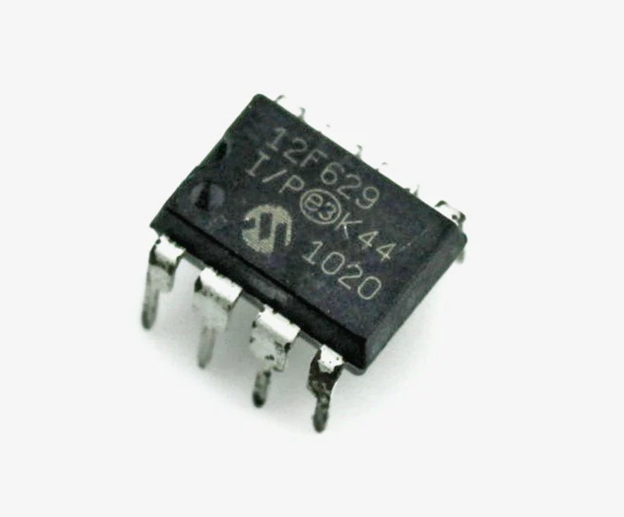
At [Your Company Name], we offer expert solutions to break Microcontroller PIC12F629 program, enabling you to restore, crack, copy, or clone the internal contents of the chip—including its binary, heximal, or source code. Whether your goal is data recovery, device duplication, or in-depth reverse engineering, we help you retrieve valuable program files, EEPROM, and flash archives locked within the device.
This microcontroller is a trusted component in a wide range of embedded systems, including:
- Remote controls
- Home automation devices
- Industrial sensor modules
- Simple logic control circuits
- Low-power portable electronics
Its built-in features like an internal oscillator, low-voltage programming, 1K word flash memory, and 128 bytes of EEPROM make it ideal for applications requiring minimal external components. However, these same benefits often make it a challenge when the device becomes secured or inaccessible.
Break Microcontroller PIC12F629 locked memory and recover Program in the format of heximal from MCU by cracking MCU tamper resistance system and copy the code to blank MCU;
High-Performance RISC CPU:
· Only 35 Instructions to Learn
– All single-cycle instructions except branches
· Operating Speed:
– DC – 20 MHz oscillator/clock input when Break Microcontroller
– DC – 200 ns instruction cycle
· Interrupt Capability
· 8-Level Deep Hardware Stack
· Direct, Indirect, and Relative Addressing modes
Special Microcontroller Features:
· Internal and External Oscillator Options
– Precision Internal 4 MHz oscillator factory calibrated to ±1%
– External Oscillator support for crystals and resonators
– 5 ms wake-up from Sleep, 3.0V, typical
· Power-Saving Sleep mode
· Wide Operating Voltage Range – 2.0V to 5.5V
· Industrial and Extended Temperature Range
· Low-Power Power-on Reset (POR)
· Power-up Timer (PWRT) and Oscillator Start-up Timer (OST)
· Brown-out Detect (BOD)
· Watchdog Timer (WDT) with Independent Oscillator for Reliable Operation
· Multiplexed MCLR/Input Pin
· Interrupt-on-Pin Change
· Individual Programmable Weak Pull-ups
· Programmable Code Protection
· High Endurance Flash/EEPROM Cell
– 100,000 write Flash endurance
– 1,000,000 write EEPROM endurance
– Flash/Data EEPROM Retention: > 40 years
Low-Power Features:
· Standby Current:
– 1 nA @ 2.0V, typical
· Operating Current:
– 8.5 mA @ 32 kHz, 2.0V, typical
– 100 mA @ 1 MHz, 2.0V, typical
· Watchdog Timer Current
– 300 nA @ 2.0V, typical
· Timer1 Oscillator Current:
– 4 mA @ 32 kHz, 2.0V, typical
Peripheral Features:
· 6 I/O Pins with Individual Direction Control
· High Current Sink/Source for Direct LED Drive
· Analog Comparator module with:
– One analog comparator
– Programmable on-chip comparator voltage reference (CVREF) module
– Programmable input multiplexing from device inputs
– Comparator output is externally accessible
· Analog-to-Digital Converter module (PIC12F675):
– 10-bit resolution
– Programmable 4-channel input
– Voltage reference input
· Timer0: 8-Bit Timer/Counter with 8-Bit Programmable Prescaler
· Enhanced Timer1:
– 16-bit timer/counter with prescaler
– External Gate Input mode
– Option to use OSC1 and OSC2 in LP mode as Timer1 oscillator, if INTOSC mode selected
· In-Circuit Serial ProgrammingTM (ICSPTM) via two pins
Many manufacturers implement code protection bits on the PIC12F629 to prevent unauthorized access. Once enabled, these protections block conventional reading or copying methods. If the chip becomes corrupted, or you’ve lost the original firmware, regaining access to your system’s logic can seem impossible.
That’s where our hack, decode, and decrypt service shines. We use specialized hardware techniques and custom tools to bypass these protections and open the memory contents of the chip. Our team can extract and reconstruct a clean, usable heximal file, ready for analysis, backup, or duplication.
Our Services Include:
- Dumping and recovering protected flash and EEPROM
- Disassembling and decoding obfuscated or encrypted firmware
- Reconstructing source code or binary files from extracted program archives
- Cloning the chip’s logic into new devices for manufacturing or system restoration
- Secure and confidential handling of client devices and data
We approach each project with precision, ensuring successful retrieval of critical information without damaging your hardware. Whether your device is part of a legacy product line or a recently developed system, we adapt our methods accordingly.
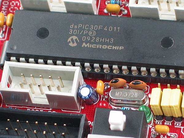
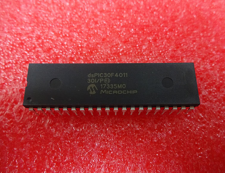
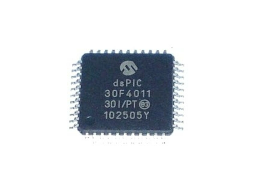
Break MCU dsPIC30F4011 Heximal
The dsPIC30F4011 stands out due to its robust motor control features, including a high-speed PWM module, a dedicated motor control DSP engine, and multiple analog inputs. It’s favored in complex systems requiring real-time control and digital signal processing. Its protected memory design and built-in code protection features make it extremely difficult for unauthorized access, yet our techniques are built to overcome these barriers legally and ethically for rightful owners.
Our Capabilities: Reverse Engineering at the Hex Level
We offer a full-service solution to break, unlock, and extract the original heximal or binary file from a secured dsPIC30F4011. Our process involves:
- Disassembling and decoding memory architecture to gain access to protected areas.
- Decrypting secured blocks of flash or EEPROM.
- Reconstructing the program file into editable and compilable source code (where feasible).
- Providing cloning or duplication of the original firmware for use in replacement MCUs or system upgrades.
Whether the firmware is lost, corrupted, or needs to be modified without original source access, we help clients recover what they need with high accuracy.
Why Clients Choose Us
- Deep Expertise: Years of experience with Microchip microcontrollers, especially dsPIC family.
- Advanced Tools: We utilize a mix of proprietary hardware and software to access and process even the most secured memory regions.
- Confidentiality Assured: Every case is handled under strict NDAs, ensuring data privacy and intellectual property protection.
- Client-Centered Approach: From motor control firms to academic researchers, we tailor our services based on the actual needs of our clients.
Real-World Applications
Many users approach us when dealing with discontinued products, broken systems, or third-party devices that are no longer supported. Breaking the MCU dsPIC30F4011 heximal allows them to continue using or replicating critical systems—whether it’s industrial drives, robotic platforms, or power converters.
Conclusion
Recovering or cloning the firmware from a secured dsPIC30F4011 is not impossible—when done by the right hands. Our specialized service empowers clients to regain access to locked program files, ensuring operational continuity, custom development, or forensic analysis. If you need to unlock, hack, or duplicate your Microchip dsPIC30F4011 data, contact us today and let our experts handle the complex job with confidence and precision.
Break MCU dsPIC30F4011 memory and extract its Heximal out from its flash and eeprom, clone firmware to blank Microcontroller dsPIC30F4011 which will provide the same functions as original IC Clone;
Peripheral Features:
this group of dsPIC30F devices and is not intended to be a complete reference source. For more information on the CPU, peripherals, register descriptions and general device functionality, refer to the “dsPIC30F Family Reference Manual” (DS70046). For more information on the device instruction set and programming, refer to the “16-bit MCU and DSC Reference Manual” (DS70157).
High-Performance, Modified RISC CPU:
· Modified Harvard architecture
· C compiler optimized instruction set architecture with flexible addressing modes
· 83 base instructions
· 24-bit wide instructions, 16-bit wide data path
· 48 Kbytes on-chip Flash program space (16K instruction words)
· 2 Kbytes of on-chip data RAM
· 1 Kbyte of nonvolatile data EEPROM
· Up to 30 MIPS operation:
– DC to 40 MHz external clock input
– 4 MHz-10 MHz oscillator input with PLL active (4x, 8x, 16x)
· 30 interrupt sources:
– Three external interrupt sources
– Eight user-selectable priority levels for each
· High-current sink/source I/O pins: 25 mA/25 mA
· Timer module with programmable prescaler:
– Five 16-bit timers/counters; optionally pair 16-bit timers into 32-bit timer modules
· 16-bit Capture input functions
· 16-bit Compare/PWM output functions
· 3-wire SPI modules (supports 4 Frame modes)
· I2C™ module supports Multi-Master/Slave mode and 7-bit/10-bit addressing
· Two UART modules with FIFO Buffers
· CAN module, 2.0B compliant
Motor Control PWM Module Features:
· Six PWM output channels:
– Complementary or Independent Output modes
– Edge and Center-Aligned modes
· Three duty cycle generators
· Dedicated time base
· Programmable output polarity
· Dead-time control for Complementary mode
· Manual output control
· Trigger for A/D conversions
Quadrature Encoder Interface Module Features:
interrupt source
– Four processor trap sources
· 16 x 16-bit working register array
Phase A, Phase B and Index Pulse input 16-bit up/down position counter
Count direction status
Position Measurement (x2 and x4) mode
Programmable digital noise filters on inputs
Dual data fetch
Accumulator write-back for DSP operations
Alternate 16-bit Timer/Counter mode
Interrupt on position counter rollover/underflow
Modulo and Bit-Reversed Addressing modes
Two, 40-bit wide accumulators with optional saturation logic
Analog Features:
· 17-bit x 17-bit single-cycle hardware fractional/integer multiplier
· All DSP instructions are single cycle
· ±16-bit, single-cycle shift
· 10-bit Analog-to-Digital Converter (ADC) with four Sample and Holde (S&H) inputs:
– 1 Msps conversion rate
– Nine input channels
– Conversion available during Sleep and Idle
· Programmable Brown-out Reset only
Break IC STM32F101C4T6TR Binary
The STM32F101C4T6TR is a widely-used ARM Cortex-M3 based microcontroller from STMicroelectronics, known for its low power consumption and powerful real-time performance in cost-sensitive embedded systems. Frequently integrated in industrial control units, medical instruments, automotive devices, and portable electronics, this MCU often contains crucial application-specific firmware that is locked or encrypted within its secured flash memory.
At CIRCUIT ENGINEERING CO.,LTD, we offer a highly specialized service to Break IC STM32F101C4T6TR Binary, enabling clients to gain access to protected or inaccessible firmware stored inside this chip. Whether your goal is to restore, clone, duplicate, or recover original firmware from the flash or EEPROM memory, our expert engineers are equipped with advanced tools and know-how to safely and efficiently extract the binary or heximal file.
Manufacturers often lock or encrypt the internal program memory of MCUs like the STM32F101C4T6TR to protect intellectual property or prevent unauthorized duplication. However, end-users or system integrators may require access to the original program or source code for legitimate reasons, including:
- Replacing damaged or lost firmware
- Upgrading or migrating legacy systems
- Debugging malfunctioning devices
- Performing third-party audits or system analysis
Our solution offers a reliable way to decode, decrypt, or crack these secured binaries and convert them into usable forms such as disassembled assembly listings or partial C-level reconstruction.
Break IC STM32F101C4T6TR memory and extract the binary or heximal out from the MCU flash and eeprom, duplicate the code to other new blank microcontroller STM32F101C4T6 which will provide the same functions;
The STM32F101C4T6TR belongs to the STM32 Value Line family, offering a cost-effective solution with the following features:
- 48 MHz ARM Cortex-M3 core
- 16 KB Flash memory and 4 KB SRAM
- Multiple I/O ports, timers, USARTs, ADCs
- Power-efficient modes for battery-operated systems
- Embedded system protection features like read-out protection (ROP)
This combination makes it ideal for use in:
- Digital metering systems
- Low-power IoT sensors
- Communication gateways
- Smart controllers and industrial machinery
Unfortunately, once the read-out protection is enabled, retrieving the program from the internal flash becomes nearly impossible without expert intervention.
Features
Core: ARM 32-bit Cortex™-M3 CPU
– 36 MHz maximum frequency, 1.25 DMIPS/MHz (Dhrystone 2.1) performance at 0 wait state memory
– Single-cycle multiplication and hardware division Up to 5 timers
– Up to two16-bit timers, each with up to 4 Memories
– 16 to 32 Kbytes of Flash memory
– 4 to 6 Kbytes of SRAM Clock, reset and supply management IC/OC/PWM or pulse counter
– 2 watchdog timers (Independent and Window)
– SysTick timer: 24-bit downcounter
– 2.0 to 3.6 V application supply and I/Os
– POR, PDR and programmable voltage detector (PVD)
– 4-to-16 MHz crystal oscillator
– Internal 8 MHz factory-trimmed RC
– Internal 40 kHz RC
– PLL for CPU clock
– 32 kHz oscillator for RTC with calibration Up to 4 communication interfaces
– 1 x I2C interface (SMBus/PMBus)
– Up to 2 USARTs (ISO 7816 interface, LIN, IrDA capability, modem control)
– 1 × SPI (18 Mbit/s) CRC calculation unit, 96-bit unique ID
Device summary
– Sleep, Stop and Standby modes
– VBAT supply for RTC and backup registers
Reference
Part number
STM32F101C4, Debug mode
– Serial wire debug (SWD) and JTAG interfaces DMA
STM32F101x4
STM32F101x6
STM32F101R4,
STM32F101T4
STM32F101C6,
STM32F101R6,
STM32F101T6
– 7-channel DMA controller
– Peripherals supported: timers, ADC, SPIs, I2Cs and USARTs 1 × 12-bit, 1 µs A/D converter (up to 16 channels)
– Conversion range: 0 to 3.6 V
– Temperature sensor Up to 51 fast I/O ports
– 26/37/51 I/Os, all mappable on 16 external interrupt vectors and almost all 5 V-tolerant
When dealing with secured, locked, or protected MCUs, our team applies a mix of hardware-based analysis, glitching techniques, and algorithmic de-obfuscation to open the firmware archive safely. We do not rely on brute force; instead, we use intelligent and precise methods to extract, copy, and analyze the content without damaging the original device.
After recovering the binary or hex file from the STM32F101C4T6TR, we can also assist with further disassembly, partial decompilation, or memory mapping to help clients understand and reuse the firmware. From EEPROM data to runtime configurations, we provide the clarity you need to replicate or restore critical system functions.