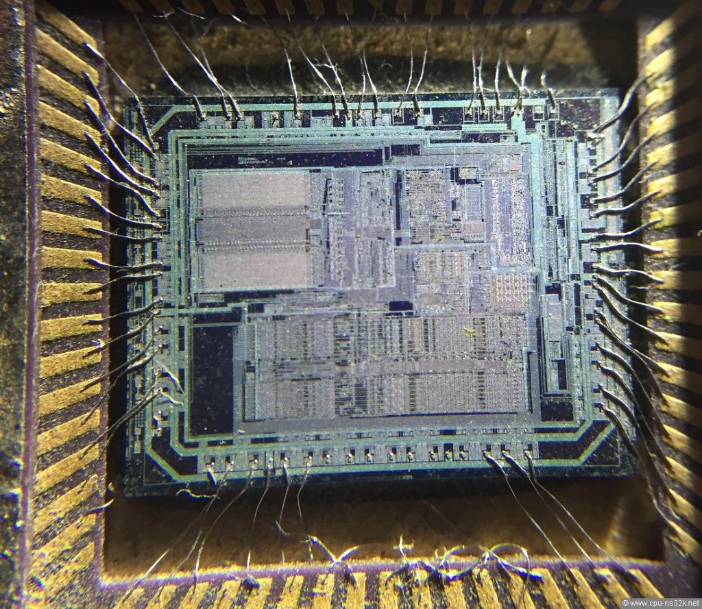
 Break dsPIC30F5016 Microchip MCU Flash Memory
Break dsPIC30F5016 Microchip MCU Flash Memory needs to Crack MCU dsPIC30F5016 security fuse bit and extract locked program from microcontroller dsPIC30F5016 flash and eeprom memory;
The core has a 24-bit instruction word. The Program Counter (PC) is 23 bits wide with the Least Significant bit (LSb) always clear (see Section 3.1 “Program Address Space”), and the Most Significant bit (MSb) is ignored during normal program execution, except for certain specialized instructions. Thus, the PC can address up to 4M instruction words of user program space.
كسر حماية نظام مقاومة العبث dsPIC30F5016 Microchip MCU واستعادة برنامج ذاكرة الفلاش بالإضافة إلى بيانات ذاكرة eeprom التي تحتاج إلى كسر وحدة التحكم الدقيقة الآمنة dsPIC30F5016 بت فتيل الأمان ونسخ الملف الثنائي المقفل أو الكود السداسي من المعالج الدقيق المضمون dsPIC30F5016؛
An instruction prefetch mechanism is used to help maintain throughput. Program loop constructs, free from loop count management overhead, are supported using the DO and REPEAT instructions, both of which are interruptible at any point to break PIC16F917 MCU memory. The working register array consists of 16×16-bit registers, each of which can act as data, address or offset registers. One working register (W15) operates as a software Stack Pointer for interrupts and calls.
dsPIC30F5016 محافظ میکروچیپ MCU سیستم مقاومت در برابر دستکاری و بازیابی برنامه فلش مموری به علاوه داده های حافظه eeprom نیاز به کرک کردن بیت فیوز امنیتی میکروکنترلر ایمن dsPIC30F5016 و کپی کردن فایل باینری قفل شده یا کد هگزیمال از dsPIC30F5016 ایمن شده با میکروپروسسور دارد.
The data space is 64 Kbytes (32K words) and is split into two blocks, referred to as X and Y data memory. Each block has its own independent Address Generation Unit (AGU). Most instructions operate solely through the X memory AGU, which provides the appearance of a single unified data space. The Multiply-Accumulate (MAC) class of dual source DSP instructions operate through both the X and Y AGUs, splitting the data address space into two parts (see Section 3.2 “Data Address Space”). The X and Y data space boundary is device specific and cannot be altered by the user.
सुरक्षात्मक dsPIC30F5016 माइक्रोचिप MCU छेड़छाड़ प्रतिरोध प्रणाली को तोड़ने और फ्लैश मेमोरी कार्यक्रम प्लस eeprom स्मृति डेटा को पुनर्प्राप्त करने के लिए सुरक्षित माइक्रोकंट्रोलर dsPIC30F5016 सुरक्षा फ्यूज बिट को तोड़ने और माइक्रोप्रोसेसर सुरक्षित dsPIC30F5016 से लॉक बाइनरी फ़ाइल या हेक्सिमल कोड की प्रतिलिपि बनाने की आवश्यकता है;
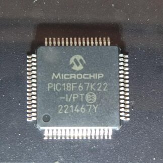
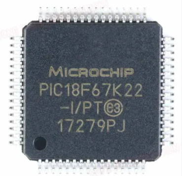
Attack PIC18F67K22 Microcontroller Memory
Attack PIC18F67K22 Microcontroller Memory can help engineer to disable the protection of MCU, and embedded binary from PIC18F67K22 MCU will be unlocked and extracted;
All of the devices in the PIC18F67K22 family offer different oscillator options, allowing users a range of choices in developing application hardware. These include:
· A Phase Lock Loop (PLL) frequency multiplier, available to the external oscillator modes which allows clock speeds of up to 64 MHz. PLL can also be used with the internal oscillator.
· An internal oscillator block that provides a 16 MHz clock (±2% accuracy) and an INTRC source (approximately 31 kHz, stable over temperature and VDD)
The PIC18F67K22 family provides ample room for application code, from 32 Kbytes to 128 Kbytes of code space. The Flash cells for program memory are rated to last up to 10,000 erase/write cycles. Data retention without refresh is conservatively estimated to be greater than 40 years.
saldırı şifreli MICROCHIP PIC18F67K22 mikrodenetleyici flash belleği ve eeprom belleği, mühendisin koruyucu PIC18F67K22 MCU’nun korumasını devre dışı bırakmasına yardımcı olabilir ve orijinal ana mikroişlemci PIC18F67K22’den gelen ikili dosyanın veya onaltılık verilerin gömülü aygıt yazılımının kilidi açılacak ve çıkarılacaktır;
The Flash program memory is readable and writable. During normal operation, the PIC18F87K22 family also provides plenty of room for dynamic application data with up to 3,862 bytes of data RAM. Should 128 Kbytes of memory be inadequate for an application, the 80-pin members of the PIC18F87K22 family have an External Memory Bus (EMB) enabling the controller’s internal program counter to address a memory space of up to 2 Mbytes. This is a level of data access that few 8-bit devices can claim and enables:
атака зашифрованная флэш-память микроконтроллера MICROCHIP PIC18F67K22 и память EEPROM могут помочь инженеру отключить защиту защитного микроконтроллера PIC18F67K22, а встроенная прошивка двоичного файла или шестнадцатеричных данных из исходного главного микропроцессора PIC18F67K22 будет разблокирована и извлечена;
The PIC18F67K22 family implements the optional extension to the PIC18 instruction set, adding eight new instructions and an Indexed Addressing mode. Enabled as a device configuration option, the extension has been specifically designed to optimize re-entrant application code originally developed in high-level languages, such as ‘C’.
ataque criptografado à memória flash do microcontrolador MICROCHIP PIC18F67K22 e à memória eeprom pode ajudar o engenheiro a desativar a proteção do MCU protetor PIC18F67K22, e o firmware incorporado do arquivo binário ou dados heximais do microprocessador mestre original PIC18F67K22 será desbloqueado e extraído;
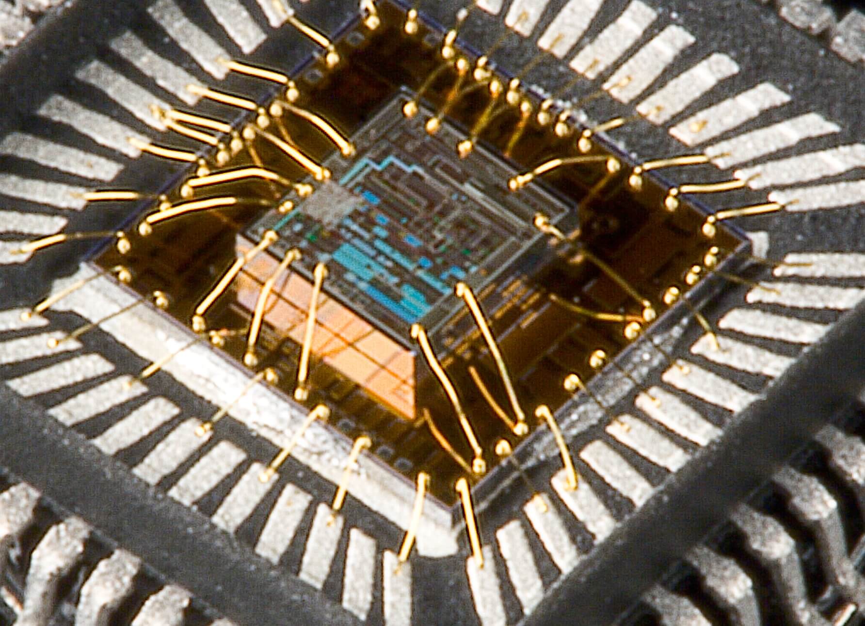
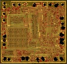
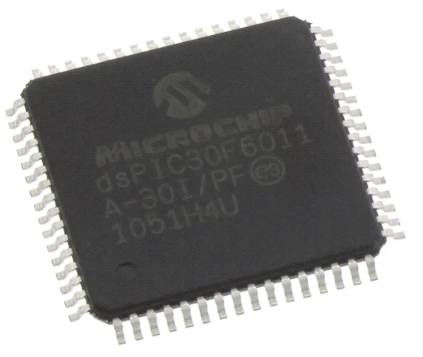
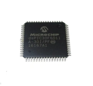
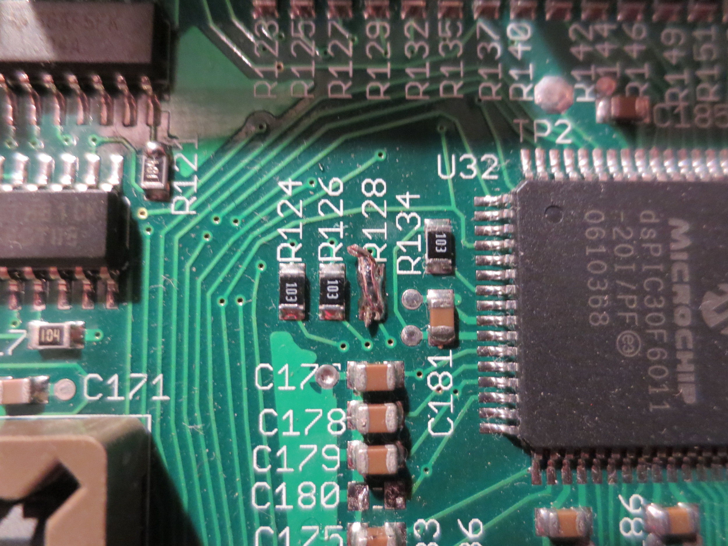
Attack Microchip dsPIC30F6011 Flash Memory
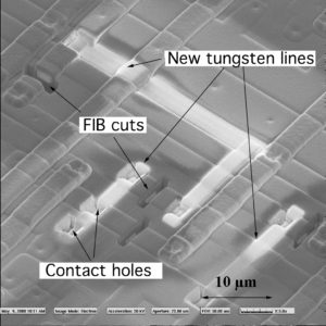
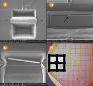
Attack Microchip dsPIC30F6011 Flash tamper resistance system and extracted heximal from locked microcontroller dsPIC30F6011, MCU dsPIC30F6011 cracking will require to use focus ion beam technique;
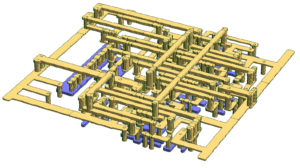
This document contains specific information for the dsPIC30F6011/6012/6013/6014 Digital Signal Controller (DSC) devices. The dsPIC30F devices contain extensive Digital Signal Processor (DSP) functionality within a high-performance 16-bit microcontroller (MCU) architecture. Figure 1-1 and Figure 1-2 show device block diagrams for dsPIC30F6011/6012 and dsPIC30F6013/6014 respectively.
This section contains a brief overview of the CPU architecture of the dsPIC30F. For additional hardware and programming information, please refer to the “dsPIC30F Family Reference Manual” (DS70046) and the “dsPIC30F/33F Programmer’s Reference Manual” (DS70157) respectively.
Mikroçip koruyucu mikrodenetleyici dsPIC30F6011 kurcalamaya karşı dayanıklılık sistemini kırın ve kilitli güvenli mikroişlemci dsPIC30F6011’den ikili dosya veya onaltılı veri formatında gömülü ürün yazılımını çıkarın, şifrelenmiş MCU dsPIC30F6011 tersine mühendislik, odak iyon ışın tekniğini kullanmayı gerektirecektir.
The core has a 24-bit instruction word. The Program Counter (PC) is 23 bits wide with the Least Significant bit (LSb) always clear (refer to Section 3.1 “Program Address Space”), and the Most Significant bit (MSb) is ignored during normal program execution, except for certain specialized instructions.
Thus, the PC can address up to 4M instruction words of user program space. An instruction prefetch mechanism is used to help maintain throughput. Program loop constructs, free from loop count management overhead, are supported using the DO and REPEAT instructions, both of which are interruptible at any point in the process of attacking encrypted mcu code.
Взлом защитного микроконтроллера микрочипа dsPIC30F6011, система защиты от несанкционированного доступа и извлечение встроенной прошивки в формате двоичного файла или шестнадцатеричных данных из заблокированного защищенного микропроцессора dsPIC30F6011, зашифрованный микроконтроллер dsPIC30F6011, обратный инжиниринг потребует использования техники фокусировки ионного луча.
The working register array consists of 16 x 16-bit registers, each of which can act as data, address or offset registers. One working register (W15) operates as a software Stack Pointer for interrupts and calls. The data space is 64 Kbytes (32K words) and is split into two blocks, referred to as X and Y data memory.
Hackear el microcontrolador de seguridad del microchip dsPIC30F6011, el sistema antimanipulación y extraer firmware en un archivo binario o datos hexadecimales del microprocesador de seguridad dsPIC30F6011 bloqueado, el microcontrolador cifrado dsPIC30F6011 y la ingeniería inversa requerirán el uso de una técnica de enfoque de haz de iones.
The upper 32 Kbytes of data space memory can be mapped into the lower half (user space) of program space at any 16K program word boundary, defined by the 8-bit Program Space Visibility Page (PSVPAG) register. This lets any instruction access program space as if it were data space, with a limitation that the access requires an additional cycle. Moreover, only the lower 16 bits of each instruction word can be accessed using this method.
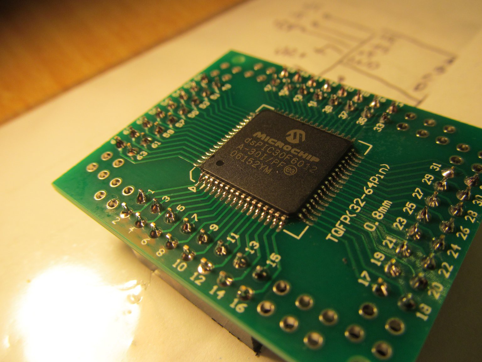
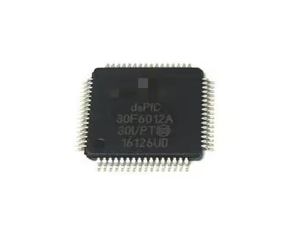
Break MCU dsPIC30F6012 Memory
Break MCU dsPIC30F6012 Memory security fuse bit, then copy embedded heximal from locked microcontroller dsPIC30F6012 flash and eeprom memory, microcontroller dsPIC30F6012 protection cracking will be relied on the focus ion beam technology;
DOSTART, DOEND, DCOUNT shadows are pushed on loop start, and popped on loop end. When a byte operation is performed on a working register, only the Least Significant Byte (LSB) of the target register is affected. However, a benefit of memory mapped working registers is that both the Least and Most Significant Bytes can be manipulated through byte wide data memory space accesses.
Some of these registers have a shadow register associated with each of them, as shown in Figure 2-1. The shadow register is used as a temporary holding register and can transfer its contents to or from its host register upon the occurrence of an event. None of the shadow registers are accessible directly.
quebre o bit de fusível de segurança de memória flash MCU dsPIC30F6012 protetor e, em seguida, duplique o código heximal incorporado ou arquivo binário do microcontrolador bloqueado dsPIC30F6012 memória flash e eeprom, microprocessador criptografado a quebra de proteção dsPIC30F6012 será baseada na tecnologia de feixe de íons de foco
The following rules apply for transfer of registers into and out of shadows. The dsPIC® DSC devices contain a software stack. W15 is the dedicated software Stack Pointer (SP), and will be automatically modified by exception processing and subroutine calls and returns. However, W15 can be referenced by any instruction in the same manner as all other W registers which can help to recover IC embedded firmware.
złam ochronny bezpiecznik pamięci flash MCU dsPIC30F6012, następnie zduplikuj osadzony kod szesnastkowy lub plik binarny z zablokowanej pamięci flash i eeprom mikrokontrolera dsPIC30F6012, zaszyfrowany mikroprocesor Ochrona przed pękaniem dsPIC30F6012 będzie opierać się na technologii skupionej wiązki jonów
This simplifies the reading, writing and manipulation of the Stack Pointer (e.g., creating stack frames). The dsPIC DSC core has a 16-bit STATUS register (SR), the LSB of which is referred to as the SR Low byte (SRL) and the Most Significant Byte (MSB) as the SR High byte (SRH). See Figure 2-1 for SR layout.
Cassez le bit de fusible de sécurité de la mémoire flash du MCU dsPIC30F6012 de protection, puis dupliquez le code heximal intégré ou le fichier binaire à partir de la mémoire flash et eeprom du microcontrôleur verrouillé dsPIC30F6012, la protection cryptée du microprocesseur dsPIC30F6012 sera basée sur la technologie de faisceau d’ions de mise au point.
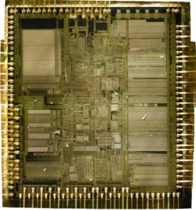
Recover MCU Layout Design Infringement
Recover MCU Layout Design without the consent of the right holder constitutes an infringement. There are two main types of microcontroller copying here, one is full replication, the other is partial replication.
The illegal copying of other people’s mcu layout designs will infringe on the continuous development of the integrated circuit industry and thus harm the public’s interests. A semiconductor manufacturer may have to spend millions of dollars to develop semiconductor chips, but a pirate company may need to spend hundreds of thousands of dollars to clone IC, so the pirate company can sell it at a lower price. Such chips have caused huge losses to manufacturers who develop chips.
Recover MCU Layout Design Infringement
This kind of illegal competition is extremely harmful to the sustainable development of the semiconductor industry. Therefore, it is necessary to crack down on this behavior, but the premise is that it can correctly identify such plagiarism and copying behavior in practice.
PLD Chip Reverse Engineering
In the case that property holder and defendant are competitors in the semiconductor industry. The property holder produced a PLD (Programmable Logic Device) chip to perform various logic functions. defendant produces different types of chips, called ASIC (Application-Specific Integrated Circuit), which performs different functions than the property holder’s chip. However, the property holder believes that the layout design of the chip ASIC produced by the defendant (called the mask work in the United States) duplicated layout design that he registered which is obtained from PLD Chip Reverse Engineering.
PLD Chip Reverse Engineering
PLD Chip Reverse Engineering clause on the one hand protects the interests of the owner of the layout design and on the other hand promotes technological innovation. In PLD reverse engineering, the second layout design must not be substantially the same as the first layout design.
As long as there is evidence that substantial investment and effort has been made in the development of the update new layout design, not just 100% cloning, it does not constitute infringement, even if the two layout designs are similar in some substantive parts.
The law actually allows competitors to copy microcontroller layout designs, but only if the purpose of reproduction is to develop their own original layout design.
As long as a PLD layout design embodies a low degree of creativity in any aspect, it can be considered original, and the requirements for creativity here are quite low.
In the Microcontroller reverse engineering process, competitors can take pictures and copy the registered layout design, but if competitors use this information to produce a substantially identical layout design, then it cannot be called legal reverse engineering. 1 Legal reverse engineering refers to taking pictures and copying layout designs, but the purpose of photographing and copying is to analyze the research, and combine the results of analysis and research into their own layout design to generate unique and genuine Layout design.
Breaking Original IC Layout Design
A prerequisite for the establishment of Breaking Original IC Layout Design defense is that the new layout design must be original compared to the prior layout design, and judging whether it is original or not is largely based on facts.
Breaking Original IC Layout Design
The court also held that if the replica of the IC layout design did have the intention of reverse engineering at first, but ultimately failed, then the law could not exempt his tort liability.
The written clues can prove to some extent that the layout design owner has independently created, but can not completely determine the originality of the layout design, and can not completely determine that the layout design is not acquired from Cloning IC layout design;
The Court of Appeals suggested that AMD did not use other alternative transistor configurations, but instead used the configuration of Brooktree, so it can be inferred that when infringer Breaking Original IC Layout Design of the owner chip, it did not design the layout itself, but just copied owner’s layout, so there is no way to assume that infringer is doing reverse engineering microcontroller. The court finally ruled that the defense of infringer reverse engineering is not established, and infringer constitutes infringement.
Reverse Engineering Microcontroller Layout Design
Infringer further argued that Reverse Engineering Microcontroller Layout Design on the core unit of the copyright holder layout design. It proposes that, according to the law, if the microcontroller layout design is developed through reverse engineering, then it is not necessary to bear the tort liability.
Reverse Engineering Microcontroller Layout Design
In the instructions given to the jury, the court pointed out that if the non-rights person reverse engineered and studied the layout design of others’ microcontroller, analyzed the circuit structure, and then integrated the analysis results into his own layout design, it did not constitute infringement.
The instructions emphasize that if infringer’s layout design contains its own new design elements, an improvement or an alternative to the copyright holder layout design, then the layout design is original.
It also explains that the layout design obtained through reverse engineering can be considered as original and therefore does not constitute infringement, but only if it is not substantially similar to the protected layout design, and its design contains significant Hard work and commitment, not just copying.
The instructions also remind the jury to focus on whether the defendant’s layout design is an original microcontroller layout design obtained through reverse engineering.
Infringer pointed out that it has made a lot of investment in the process of developing microcontroller layout design, and the Semiconductor Chip Protection Act prohibits the investment of very small plagiarism, rather than the reverse engineering behavior that has invested a lot of time and energy.
It also presented a paper trail to prove that it was a mcu reverse engineering rather than a simple microcontroller copy. Infringer has always stressed that he has no intention of copying copyright holder’s layout design, and he has not done so. As can be seen from the written traces, Infringer spent more than $3 million and two and a half years to analyze copyright holder’s layout design.
Infringer points out that if you want to copy copyright holder’s layout design, it only takes a few months, not a few years. At the same time, Infringer proposed that its controlled semiconductor chip is smaller and faster than copyright holder’s chip.
MCU Reverse Engineering Process
In the development of the integrated circuit industry, MCU reverse engineering plays a huge role in promoting the faster design of MCU products with the same basic functions but better performance, smaller size and lower cost.
Integrated circuit technology is one of the fastest growing and most dynamic technologies in the world. With the continuous improvement of the performance of integrated circuits, the functions are continuously enhanced, and the application surface is expanding. The integrated circuit industry has become a pillar industry of the national economy and has become a driving force. One of the main factors in the world of today’s information society.
MCU Reverse Engineering Process
Experience has shown that it takes three years or longer time to completely develop a new microcontroller independently, and it takes one years or more to redesign MCU from the circuitry pattern which has been obtained from MCU reverse engineering process;
If it is MCU copied directly, It only takes three to five months. It can be seen that the application of MCU source code reverse engineering to develop Microcontrollers still requires considerable investment, so it does not deviate from the principle of fair competition.
It is precisely because of MCU reverse engineering:
1st of all, the basic principles of this technique isn’t excessively violate the fair competition. Secondly, the development of the integrated circuit industry will be vigorously promoted. Therefore, countries generally recognize MCU reverse engineering in the legislation of integrated circuits.
However, the reverse engineering is to crack MCU‘s key technology of others’ design. On the basis of this, the layout design obtained will inevitably contain the imitation and copying of the prior microcontroller layout design, so it is easy to generate infringement disputes. In the event of an infringement dispute, the accused infringer must be defended on the grounds of reverse engineering, and a series of more complicated problems will be highlighted.
Microcontroller Reverse Engineering Behavior
In the development of the Integrated circuit industry, Microcontroller Reverse Engineering behavior is common. This behavior is beneficial to designing integrated circuit products with the same basic functions but better performance, smaller size and lower cost.
The technological advancement of the integrated circuit industry does not unduly violate the principle of fair competition. Therefore, countries generally recognize the legitimacy of microcontroller reverse engineering behavior in the Integrated circuit protection law, which makes reverse engineering IC an important defense tools for integrated circuit copyright infringement.
Microcontroller Reverse Engineering Behavior
However, reverse engineering is method to dissipate and acquire the key technology of other designer (property owner). On the basis of this, the layout design obtained will inevitably contain the imitation and microcontroller copying of the prior layout design, so it is easy to be confused with the infringement, thus causing disputes.
Therefore, it is very necessary to make an accurate distinction between infringement and reverse engineering behavior. On the one hand, it helps to protect the legal rights of the owner of the layout design, avoids the infringer’s use of reverse engineering IC as a defense tool to escape legal sanctions, and on the other hand enables the person implementing reverse engineering to correctly assess the legal risk of his behavior. To understand whether it is possible to suspect infringement litigation and how to circumvent it, so that the integrated circuit industry will develop in a healthy and orderly direction.
On the basis of introducing the basic knowledge of integrated circuit, circuitry layout design and MCU reverse engineering, the article focuses on the judgment standard of integrated circuit infringement and the judgment standard of microcontroller reverse engineering behavior, thus clarifying the relationship between infringement and reverse engineering behavior.