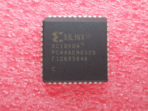
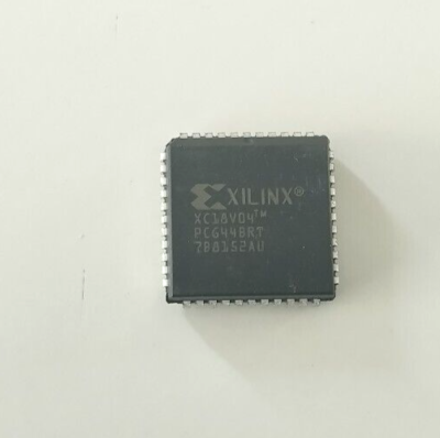
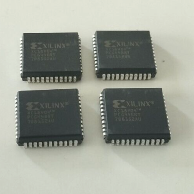
 Copy MCU XC18V04PC44C Program
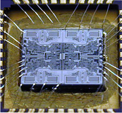
In the specialized field of reverse engineering, few tasks are as technically demanding as attempting to copy, clone, or recover program code from secured microcontrollers like the XILINX XC18V04PC44C CPLD. This complex FPGA configuration chip is often deployed in critical systems where intellectual property protection is paramount. The process of firmware extraction from such protected, encrypted, or locked devices represents the pinnacle of technical reverse engineering, requiring sophisticated methodologies to decrypt, decode, or otherwise break advanced security mechanisms without physical destruction of the component. This article explores the technical challenges, ethical considerations, and significant benefits underlying this delicate process.
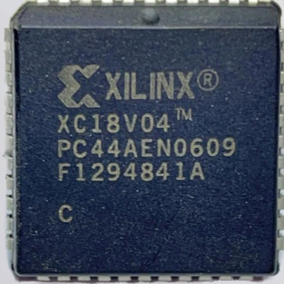
We can Copy MCU XC18V04PC44C Program, please view below MCU XC18V04PC44C features for your reference:
XILINX XC18V04PC44C: Deployment and Security Significance
The XILINX XC18V04PC44C is not a standard microcontroller but a CPLD (Complex Programmable Logic Device) specifically designed for configuration storage in high-reliability applications. This chip frequently serves critical functions across several industries:
- Telecommunications Infrastructure: Used in network routing and switching equipment for storing configuration bitstreams that define hardware functionality
- Aerospace and Defense Systems: Employed in avionics and military hardware where firmware integrity is crucial for operational safety and security
- Industrial Automation: Found in programmable logic controllers (PLCs) and manufacturing control systems
- Medical Electronics: Utilized in diagnostic and therapeutic medical devices requiring reliable configuration storage
As a non-volatile memory component, the XC18V04PC44C stores configuration data that defines the operational characteristics of associated FPGAs or other programmable logic. The secured nature of this chip prevents unauthorized access to proprietary algorithms and hardware implementations, protecting significant research and development investments embodied in the firmware
XC18V00 Series In-System-Programmable Configuration PROMs:
Product Specification:
In-System Programmable 3.3V PROMs for Configuration of Xilinx FPGAs
♦ Endurance of 20,000 Program/Erase Cycles
♦ Program/Erase Over Full Industrial Voltage and Temperature Range (–40°C to +85°C)
IEEE Std 1149.1 Boundary-Scan (JTAG) Support
JTAG Command Initiation of Standard FPGA Configuration
Simple Interface to the FPGA
Cascadable for Storing Longer or Multiple Bitstreams
Low-Power Advanced CMOS FLASH Process Dual Configuration Modes
Technical Challenges in Accessing Protected Memory
Attempting to recover, clone, or replicate the binary or heximal content from a secured XC18V04PC44C presents formidable technical obstacles that differentiate this process from simple microcontroller duplication:
- Advanced Encryption and Protection Schemes: Unlike simpler microprocessors, the XC18V04PC44C typically incorporates sophisticated security measures designed specifically to prevent firmware extraction. These may include hardware-based encryption of the configuration data, volatile key storage that disappears upon power disruption, and active tamper-detection circuits that can erase critical memory content if intrusion is detected
- Proprietary Memory Architecture: The internal flash or EEPROM memory structure of these specialized chips often differs significantly from standard microcontroller architectures. Without detailed documentation of the memory mapping and access protocols, even bypassing security does not guarantee successful interpretation of the extracted binary data
- Limited Attack Vectors: Standard reverse engineering approaches such as debug port exploitation or simple decapsulation often prove ineffective against properly implemented security in the XC18V04PC44C. The chip’s design specifically anticipates and mitigates these common attack methods, necessitating more advanced approaches
♦ Serial Slow/Fast Configuration (up to 33 MHz)
♦ Parallel (up to 264 Mb/s at 33 MHz)
5V-Tolerant I/O Pins Accept 5V, 3.3V and 2.5V Signals
3.3V or 2.5V Output Capability
Design Support Using the Xilinx ISE™ Foundation™ Software Packages
Available in PC20, SO20, PC44, and VQ44 Packages
Lead-Free (Pb-Free) Packaging
Description
Xilinx introduces the XC18V00 series of in-system programmable configuration PROMs (Figure 1). Devices in this 3.3V family include a 4-megabit, a 2-megabit, a 1-megabit, and a 512-kilobit PROM that provide an easy-to- use, cost-effective method for reprogramming and storing Xilinx FPGA configuration bitstreams. When the FPGA is in Master Serial mode, it generates a configuration clock that drives the PROM.
A short access time after CE and OE are enabled, data is available on the PROM DATA (D0) pin that is connected to the FPGA DIN pin. New data is available a short access time after each rising clock edge. The FPGA generates the appropriate number of clock pulses to complete the configuration. When the FPGA is in Slave Serial mode, the PROM and the FPGA are clocked by an external clock.
When the FPGA is in Master SelectMAP mode, the FPGA generates a configuration clock that drives the PROM. When the FPGA is in Slave Parallel or Slave SelectMAP mode, an external oscillator generates the configuration clock that drives the PROM and the FPGA.
After CE and OE are enabled, data is available on the PROM’s DATA (D0-D7) pins. New data is available a short access time after each rising clock edge. The data is clocked into the FPGA on the following rising edge of the CCLK. A free-running oscillator can be used in the Slave Parallel or Slave SelecMAP modes.
Multiple devices can be cascaded by using the CEO output to drive the CE input of the following device. The clock inputs and the DATA outputs of all PROMs in this chain are interconnected. All devices are compatible and can be cascaded with other members of the family or with the XC17V00 one-time programmable serial PROM family.