Archive for the ‘Reverse Engineer Microcontroller’ Category
 Copy Microcontroller PIC16C771 Firmware
 June 22nd, 2000 |
  Author:
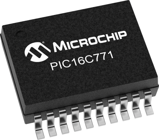
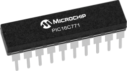
 The PIC16C771 is a notable member of Microchip’s PIC family, featuring an integrated Analog-to-Digital Converter (ADC) and a sophisticated Capture/Compare/PWM module. These features made it a popular choice for applications requiring sensor interfacing and motor control. You would often find this microprocessor at the heart of early-generation automotive control units, specialized medical diagnostic devices, and precision industrial timers. Its architecture stores the critical operational program in internal flash and EEPROM memory. To prevent unauthorized access, Microchip equipped these chips with robust code protection fuses. When enabled, these locked and secured states make directly reading out the intelligible source code impossible, turning any attempt to clone the MCU into a complex reverse engineering puzzle.
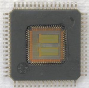
Copy Microcontroller PIC16C771 Firmware which include the program of flash memory and data of eeprom memory, disable the security fuse bit by focus MCU cracking ion beam technique, extract code from MCU PIC16C771 memory;
The Special Function Registers are registers used by the CPU and Peripheral Modules for controlling the desired operation of the microcontrollere. These registers are implemented as microcontroller RAM.
The primary difficulty in any attempt to break the protection of the PIC16C771 lies in the very nature of its security design. The goal is to obtain a perfect binary or heximal dump of the memory contents, but the protected state actively prevents this. Standard programming interfaces are rendered useless for reading the firmware file. Therefore, engineers must employ advanced, non-invasive methods to attack the security mechanism. This can involve sophisticated techniques that require deep knowledge of the chip‘s physical and logical operation.
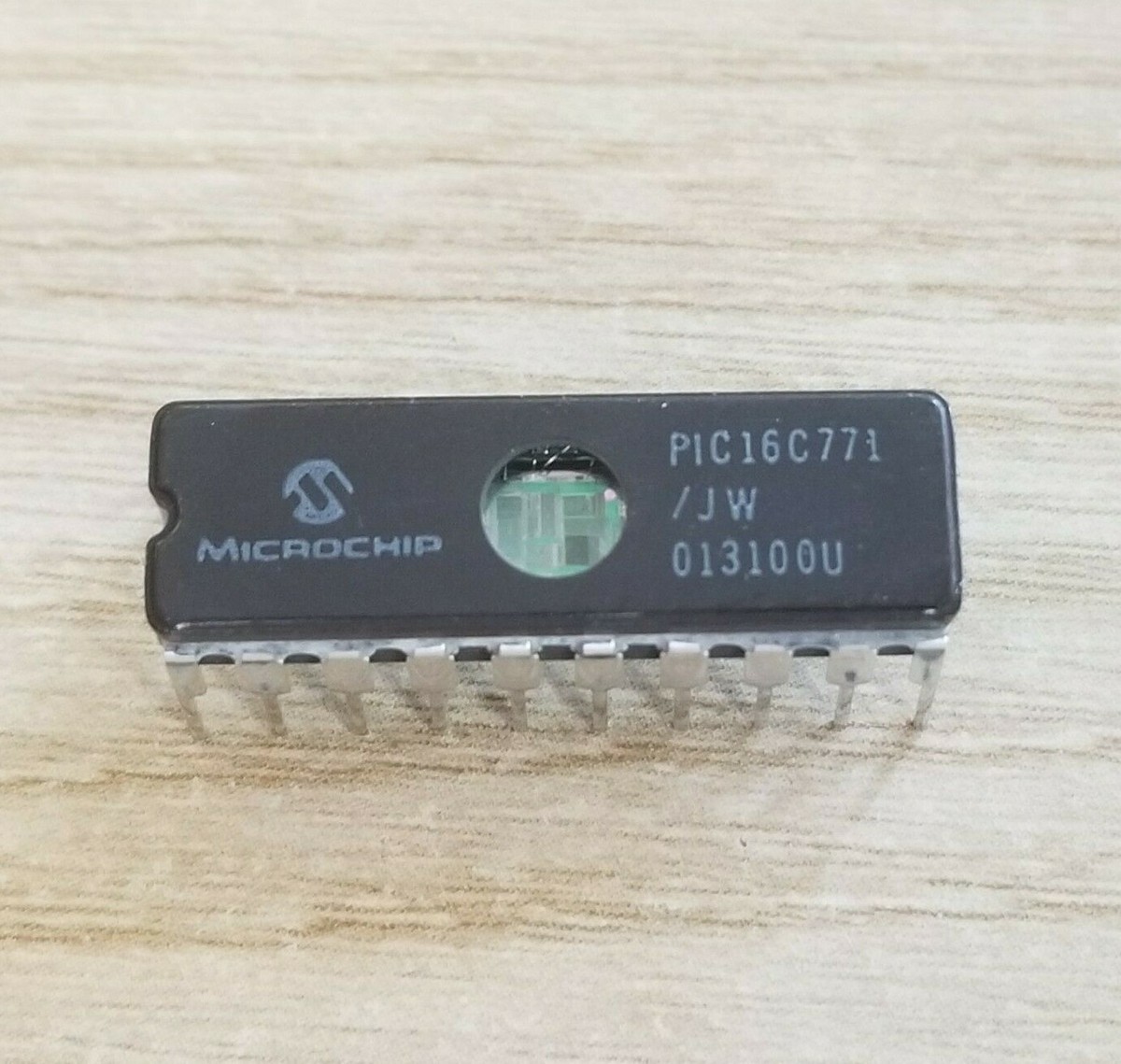
The process is not about decrypting a file in the conventional sense, as the code isn’t always encrypted but rather physically locked away by fused bits. Successfully bypassing this requires a meticulous approach to replicate the conditions under which the microcontroller relinquishes its archive of operational data.
core (CPU) and peripheral. Those registers associated with the core functions are described in detail in this section. Those related to the operation of the peripheral features are described in detail in that peripheral feature section. For example, CLRF STATUS will clear the upper-three when breaking microcontroller TMS320F28044 heximal; The STATUS register, shown in Register 2-1, contains the arithmet microcontroller status of the ALU, the RESET status and the bank select bits for data memory.
The STATUS register can be the destination for any instruction, as with any other register. If the STATUS register is the destination for an instruction that affects the Z, DC or C bits, then the write to these three bits is disabled. These bits are set or cleared according to the microcontroller log microcontroller. Furthermore, the TO and PD bits are not writable. Therefore, the result of an instruction with the STATUS register as destination may be different than intended.
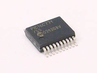
attack microprocessor PIC16C771 fuse and readout flash memory content
It is recommended, therefore, that only BCF, BSF, SWAPF and MOVWF instructions are used to alter the STATUS register, because these instructions do not affect the Z, C or DC bits from the STATUS register. For other instructions not affecting any status bits, see the ”Instruction Set Summary. when break microcontroller PIC16F886 software
The program counter (PC) specifies the address of the instruction to fetch for execution. The PC is 13 bits wide. The low byte is called the PCL register. This register is readable and writable. The high byte is called the PCH register. This register contains the PC<12:8> bits and is not directly readable or writable. All updates to the PCH register occur through the PCLATH register.
PMICROCONTROLLER16C717/770/771 microcontrolleres are capable of addressing a continuous 8K word block of program memory. The CALL and GOTO instructions provide only 11 bits of address to allow branching within any 2K program
memory page. When doing a CALL or GOTO instruction, the upper 2 bits of the address are provided by PCLATH<4:3>. When doing a CALL or GOTO instruction, the user must ensure that the page select bits are programmed so that the desired program memory page is addressed.
A return instruction pops a PC address off the stack onto the PC register. Therefore, manipulation of the PCLATH<4:3> bits are not required for the return instructions ( POPs the address from the stack).
The stack allows a combination of up to 8 program calls and interrupts to occur. The stack contains the return address from this branch in program execution. Mid-range microcontroller have an 8-level deep x 13-bit wide hardware stack.
The stack space is not part of either program or data space and the stack pointer is not readable or writable. The PC is Pushed onto the stack when a CALL instruction is executed or an interrupt causes a branch. The stack is Poped in the event of RETURN, RETLW or a RETFIE instruction execution. PCLATH is not modified when the stack is PUSHed or POPed.
After the stack has been PUSHed eight times, the ninth push overwrites the value that was stored from the first push. The tenth push overwrites the second push (and so on).
The INDF register is not a microcontroller register. Addressing INDF actually addresses the register whose address is contained in the FSR register (FSR is a pointer). This is indirect addressing.
Reading INDF itself indirectly (FSR = 0) will produce 00h. Writing to the INDF register indirectly results in a no-operation (although STATUS bits may be affected). A simple program to clear RAM locations 20h-2Fh using indirect addressing is shown in Example 2-1 Some pins for these I/O ports are multiplexed with an alternate function for the peripheral features on the microcontroller. In general, when a peripheral is enabled, that pin may not be used as a general purpose I/O pin which normally executed for cracking microcontroller pic16c771 fuse bit.
Additional information on I/O ports may be found in the microcontroller Mid-Range Reference Manual, (DS33023). PORTA is a 8-bit wide bi-directional port. The corre-analog mode of the corresponding pins. sponding data direction register is TRISA. Setting a TRISA bit (=1) will make the corresponding PORTA pin an input, i.e., put the corresponding output driver in a hi-impedance mode. Clearing a TRISA bit (=0) will make the corresponding PORTA pin an output, i.e., put the contents of the output latch on the selected pin.
Reading the PORTA register reads the status of the pins, whereas writing to it will write to the port latch. All write operations are read-modify-write operations. Therefore, a write to a port implies that the port pins are read, this value is modified, and then written to the port data latch.
Pins RA<3:0> are multiplexed with analog functions, such as analog inputs to the A/D converter, analog VREF inputs, and the on-board band gap reference outputs. When the analog peripherals are using any of Pin RA4 is multiplexed with the Timer0 module clock input to become the RA4/T0CKI pin. The RA4/T0CKI pin is a Schmitt Trigger input and an open drain output.

Pin RA5 is multiplexed with the microcontroller reset (MCLR) and programming input (VPP) functions. The RA5/ MCLR/VPP input only pin has a Schmitt Trigger input buffer. All other RA port pins have Schmitt Trigger input buffers and full CMOS output buffers. Pins RA6 and RA7 are multiplexed with the oscillator input and output functions. The TRISA register controls the direction of the RA pins, even when they are being used as analog inputs. The user must ensure the bits in the TRISA register are maintained set when using them as analog inputs.
So, why would one need to hack or reverse engineer such a component? The motivation is almost always about preservation and modernization. For our clients, the ability to recover this firmware is paramount. It allows them to restore a failed system when replacement chips or archived source code are unavailable. It enables the cloning of a functional MCU to keep a critical production line running. Furthermore, extracting this binary is the essential first step for any future project to replicate the system’s functionality on a modern, more readily available platform. The value isn’t in stealing intellectual property, but in recovering it to ensure the longevity and serviceability of vital industrial equipment, saving clients from catastrophic downtime and obsolescence.
 Posted in
Copy MCU PIC18F4685 Software
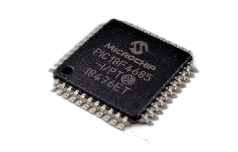
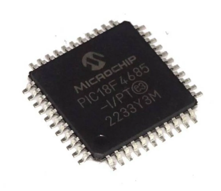
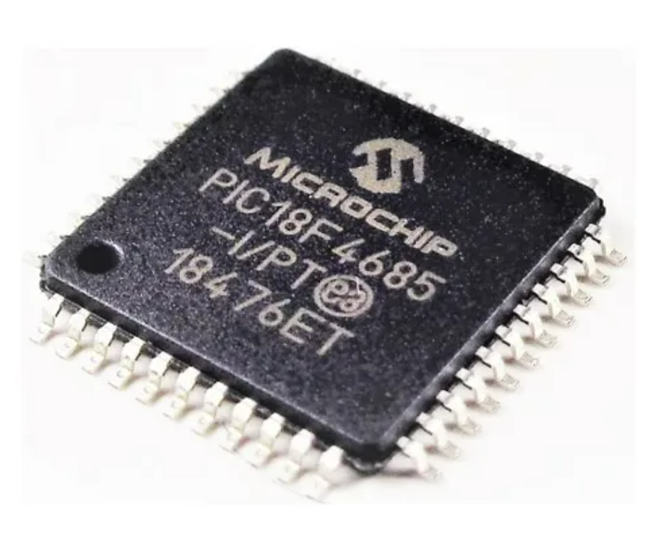
The PIC18F4685 is a powerful 8-bit microcontroller from Microchip Technology, widely adopted in automotive electronics, industrial control systems, smart devices, and other advanced embedded applications. Designed with integrated CAN communication, extended EEPROM capabilities, and a large program flash memory, this chip is known for its high-performance, secured architecture and robust data protection mechanisms.
However, when the original heximal or binary files are lost or inaccessible, it can bring development or maintenance to a standstill. Whether for legacy system restoration, product optimization, or technical auditing, customers may find themselves needing to copy MCU PIC18F4685 software from a functional device. This task can be daunting due to the chip’s locked, encrypted, or code-protected memory structure.
That’s where [Your Company Name] comes in.
Specialized Service to Recover PIC18F4685 Firmware
We provide professional, confidential services to copy, clone, or duplicate the complete contents of the MCU PIC18F4685, including program flash, EEPROM, and configuration data. Whether the device is secured, obfuscated, or encrypted, our team utilizes sophisticated hardware interfaces and reverse engineering techniques to unlock, crack, or decode the protected firmware without damaging the chip.
Through a series of non-destructive probing, memory readout, and firmware extraction processes, we can help you recover the essential heximal files, source code, or data archives needed for:
- Software backup and replication
- Faulty device replacement
- Legacy product updates
- Custom modification or migration
- Vulnerability assessment and debugging
Why the PIC18F4685 Stands Out
This Microchip MCU offers advanced features that make it ideal for complex control systems:
- 96KB of Flash program memory and 1KB EEPROM, suitable for multi-function codebases
- Integrated Enhanced CAN module for robust communication in automotive or industrial networks
- 10-bit ADC, PWM modules, and multiple timers for flexible peripheral control
- Self-write programming capability, enabling field updates
- Selective code protection to prevent unauthorized access
These features make the PIC18F4685 highly reliable but also difficult to access once the firmware is locked. This level of protection is excellent for manufacturers but presents a challenge when legitimate recovery is needed.
What We Deliver
Our service doesn’t just copy or clone memory—we deliver meaningful, usable output. You receive a verified heximal firmware file, and upon request, we can assist in disassembling or partially reverse-engineering the binary to a more human-readable form, such as assembly or annotated code.
Clients trust us for our discretion, deep technical knowledge, and ethical approach. We handle each case individually, ensuring your data and objectives remain secure throughout the process.
Conclusion
If you’re in a situation where you need to restore, decrypt, or recover a protected program file from a PIC18F4685, don’t take chances with unreliable tools or guesswork. Let our experts help you copy MCU PIC18F4685 software professionally, with accuracy and respect for your IP needs. Contact us today to learn how we can support your embedded system goals.
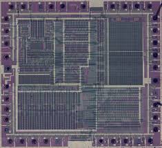
Copy MCU PIC18F4685 software inside microcontroller PIC18F4685 flash memory, decapsulate silicon package of microcontroller and get its fuse bit exposed, so MCU cracking technique will be able to reset the bit and readout the firmware from Microcontroller;
Power-Managed Modes:
Peripheral Highlights:
Run: CPU on, peripherals on
Idle: CPU off, peripherals on
Sleep: CPU off, peripherals off
Idle mode currents down to 5.8 ìA typical
Sleep mode currents down to 0.1 ìA typical
Timer1 Oscillator: 1.1 ìA, 32 kHz, 2V
Watchdog Timer: 2.1 ìA
Two-Speed Oscillator Start-up
High-Current Sink/source 25 mA/25 mA
Three External Interrupts
One Capture/Compare/PWM (CCP1) module
Enhanced Capture/Compare/PWM (ECCP1) module
(40/44-pin devices only):
– One, two or four PWM outputs
– Selectable polarity
– Programmable dead time
Flexible Oscillator Structure:
· Four Crystal modes, up to 40 MHz
· 4x Phase Lock Loop (PLL) – available for crystal and internal oscillators
· Two External RC modes, up to 4 MHz
· Two External Clock modes, up to 40 MHz
· Internal Oscillator Block:
– 8 user-selectable frequencies, from 31 kHz to 8 MHz
– Provides a complete range of clock speeds,
from 31 kHz to 32 MHz when used with PLL
– User-tunable to compensate for frequency drift
· Secondary Oscillator using Timer1 @ 32 kHz
· Fail-Safe Clock Monitor
– Allows for safe shutdown if peripheral clock stops
– Auto-shutdown and auto-restart
Master Synchronous Serial Port (MSSP) module supporting 3-Wire SPI (all 4 modes) and I2C™
Master and Slave modes
Enhanced Addressable USART module:
– Supports RS-485, RS-232 and LIN 1.3
– RS-232 operation using internal oscillator block (no external crystal required)
– Auto-wake-up on Start bit
– Auto-Baud Detect
10-Bit, up to 11-Channel Analog-to-Digital
Converter module (A/D), up to 100 ksps:
– Auto-acquisition capability
– Conversion available during Sleep
Dual Analog Comparators with Input Multiplexing
Special Microcontroller Features:
· C compiler Optimized Architecture with optional
Extended Instruction Set
· 100,000 Erase/Write Cycle Enhanced Flash
Program Memory typical
· 1,000,000 Erase/Write Cycle Data EEPROM
Memory typical
· Flash/Data EEPROM Retention: > 40 years
· Self-Programmable under Software Control
· Priority Levels for Interrupts
· 8 x 8 Single-Cycle Hardware Multiplier
· Extended Watchdog Timer (WDT):
– Programmable period from 41 ms to 131s
· Single-Supply 5V In-Circuit Serial
Programming™ (ICSP™) via two pins
· In-Circuit Debug (ICD) via two pins
· Wide operating voltage range: 2.0V to 5.5V
ECAN Module Features:
· Message bit rates up to 1 Mbps
· Conforms to CAN 2.0B ACTIVE Specification
· Fully Backward Compatible with PIC18XXX8 CAN modules
· Three Modes of Operation:
– Legacy, Enhanced Legacy, FIFO
· Three Dedicated Transmit Buffers with Prioritization
· Two Dedicated Receive Buffers
· Six Programmable Receive/Transmit Buffers
· Three Full, 29-Bit Acceptance Masks
· 16 Full, 29-Bit Acceptance Filters w/Dynamic Association
· DeviceNet™ Data Byte Filter Support
· Automatic Remote Frame Handling
· Advanced Error Management Features