Archive for the ‘Recover Chip’ Category
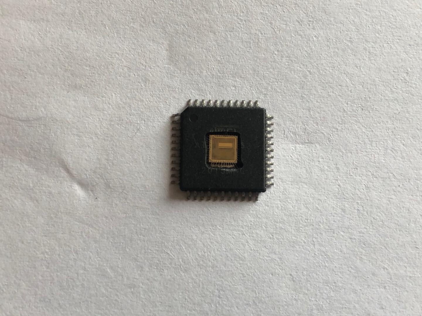
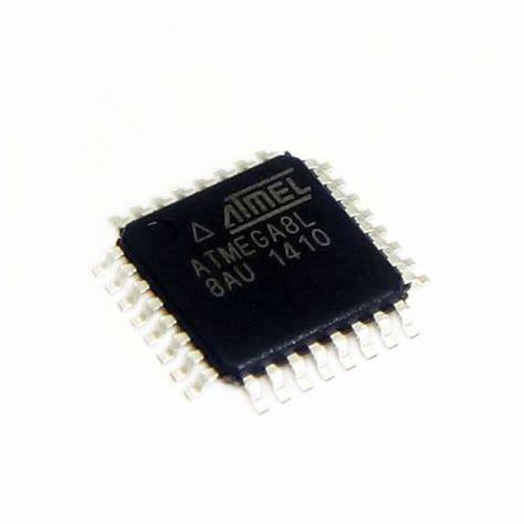
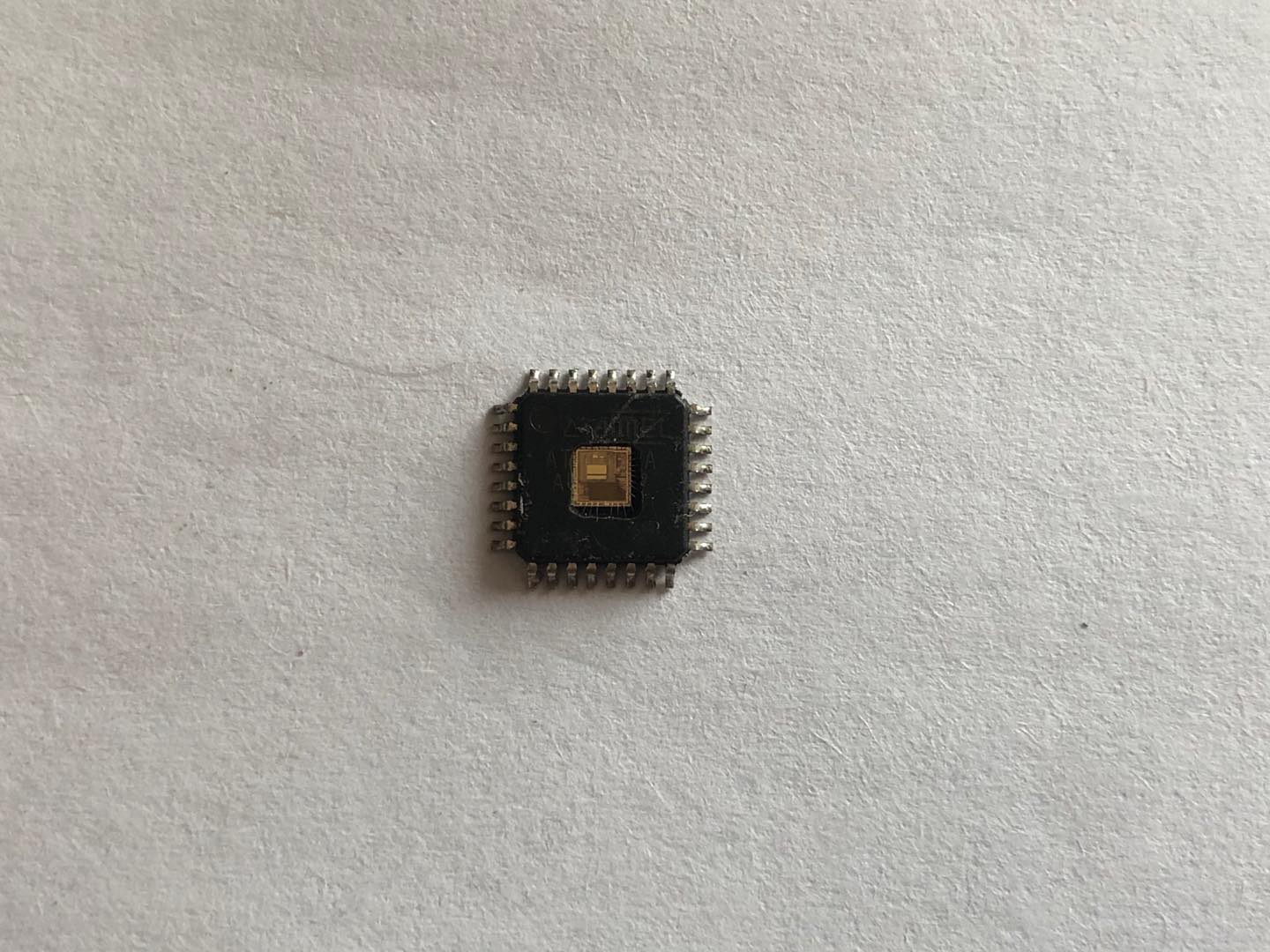
 Protective Microprocessor ATmega16 Firmware Recovery
Protective Microprocessor ATmega16 Firmware Recovery needs to crack atmega16 secured microcontroller fuse bit, read embedded heximal file out from atmega16 mcu flash and eeprom;
The lower 1120 Data memory locations address the Register File, the I/O Memory, and the internal data SRAM. The first 96 locations address the Register File and I/O Memory, and the next 1024 locations address the internal data SRAM.
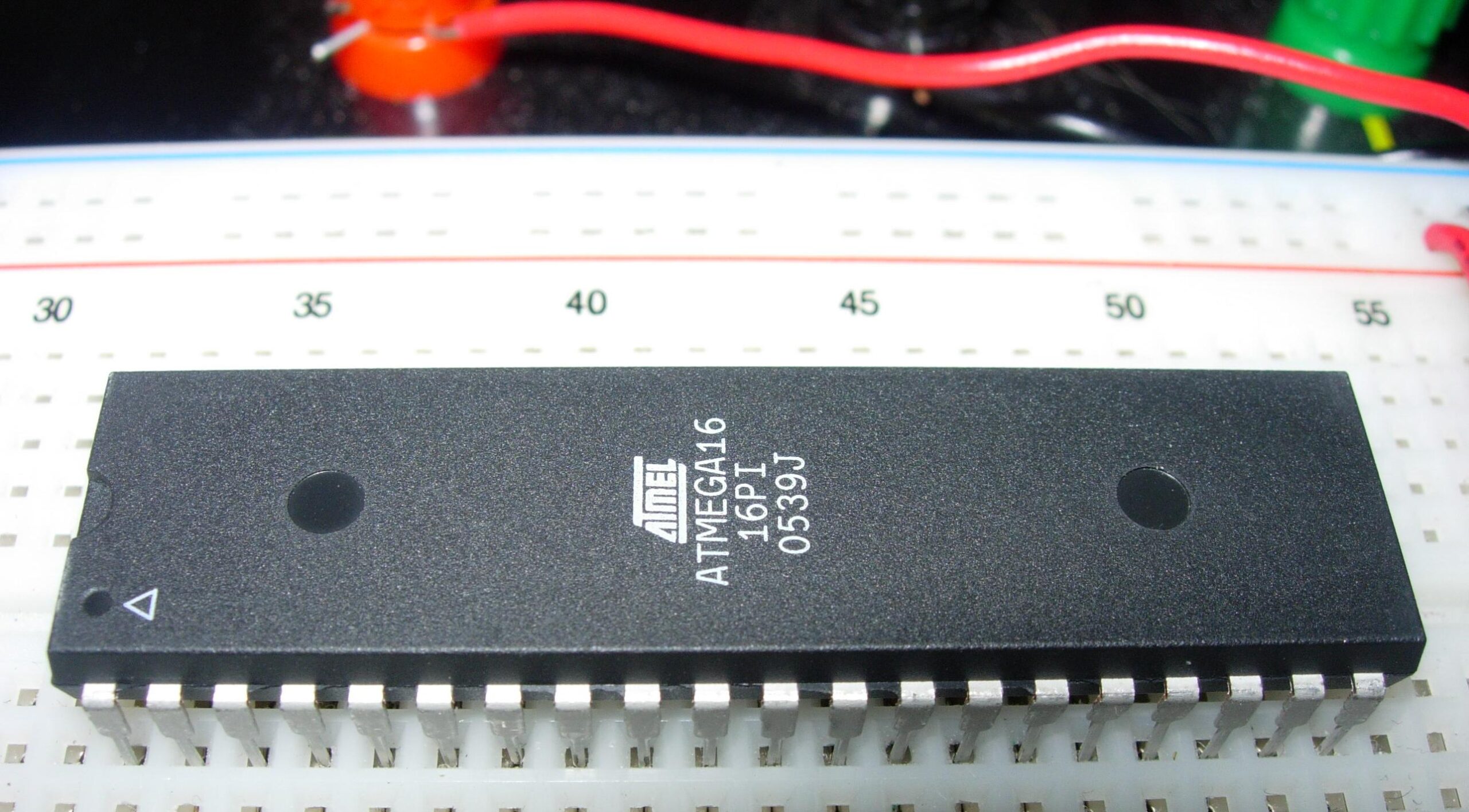
crack atmega16 locked mcu fuse bit and replicate heximal data from atmega16 microprocessor flash memory
The five different addressing modes for the Data memory cover: Direct, Indirect with Displacement, Indirect, Indirect with Pre-decrement to reverse atmega8a microchip flash memory file, and Indirect with Post-increment. In the Register File, registers R26 to R31 feature the indirect addressing pointer registers.
The direct addressing reaches the entire data space.
The Indirect with Displacement mode reaches 63 address locations from the base address given by the Y- or Z- register.
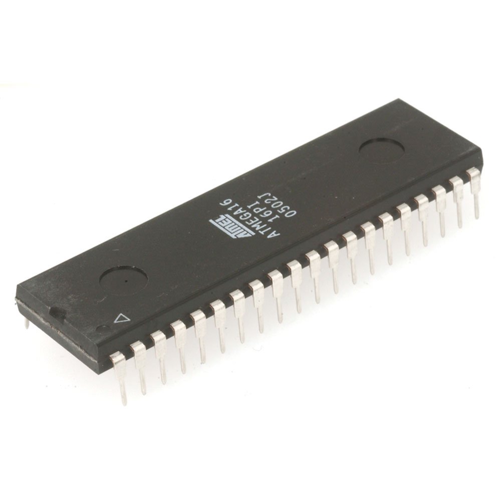
attack secured atmega16 microprocessor tamper resistance and copy embedded flash program
When using register indirect addressing modes with automatic pre-decrement and post-increment, the address registers X, Y and Z are decremented or incremented.
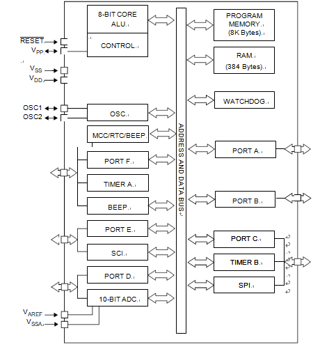
The 32 general purpose working registers, 64 I/O Registers, and the 1024 bytes of internal data SRAM in the ATmega8A are all accessible through all these addressing modes in the process of microcontroller atmega8l flash data restoration. The Register File is described in “General Purpose Register File” on page 16.
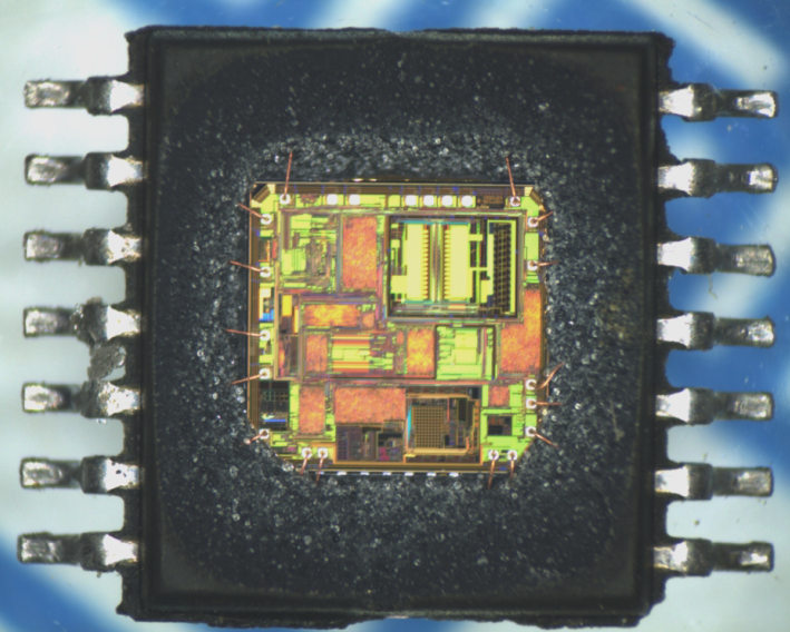
Microcontroller ATmega8L Flash Data Restoration
Microcontroller ATmega8L Flash Data Restoration is a process started from clone mcu atmega8l code from its flash memory, the embedded firmware will be readout from atmega8 microprocessor;
The Stack is effectively allocated in the general data SRAM, and consequently the Stack size is only limited by the total SRAM size and the usage of the SRAM. All user programs must initialize the SP in the reset routine (before sub-routines or interrupts are executed).
The Stack Pointer SP is read/write accessible in the I/O space. The data SRAM can easily be accessed through the five different addressing modes supported in the AVR architecture when copy mcu atmega8l heximal.
The memory spaces in the AVR architecture are all linear and regular memory maps.
microcontrolador ATmega8L restauração de dados flash é um processo iniciado a partir de clone mcu atmega8l código de sua memória flash, o firmware incorporado será lido a partir do microprocessador atmega8
A flexible interrupt module has its control registers in the I/O space with an additional global interrupt enable bit in the Status Register. All interrupts have a separate Interrupt Vector in the Interrupt Vector table.
The interrupts have priority in accordance with their Interrupt Vector position. The lower the Interrupt Vector address, the higher the priority. The I/O memory space contains 64 addresses for CPU peripheral functions as Control Registers to attack microcontroller atmega8a binary, SPI, and other I/O functions . The I/O Memory can be accessed directly, or as the Data Space locations following those of the Reg- ister File, 0x20 – 0x5F.
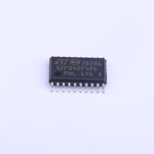
Locked STM32F050F4 Microcontroller Source Code Extraction
Crack stm32f050f4 secured mcu locked fuse bit by focus ion beam, the whole microprocessor embedded heximal copying job can be done through Locked STM32F050F4 Microcontroller Source Code Extraction.
The STM32F050xx family incorporates the high-performance ARM Cortex™-M0 32-bit RISC core operating at a 48 MHz maximum frequency, high-speed embedded memories (Flash memory up to 32 Kbytes and SRAM up to 4 Kbytes), and an extensive range of enhanced peripherals and I/Os.
All devices offer standard communication interfaces (one I2C, one SPI, one I2S, and one USART), one 12-bit ADC, up to five general-purpose 16-bit timers, a 32-bit timer and an advanced-control PWM timer to break stm32f071rb microcontroller locked bits.
The STM32F050xx family operates in the -40 to +85 °C and -40 to +105 °C temperature ranges, from a 2.0 to 3.6 V power supply. A comprehensive set of power-saving modes allows the design of low-power applications.
crack stm32f050f4 seguro mcu bloqueado fusível bit por feixe de íons de foco, todo o trabalho de cópia heximal embutida microprocessador pode ser feito através de Extração de Código Fonte do Microcontrolador Bloqueado STM32F050F4.
The STM32F050xx family includes devices in five different packages ranging from 20 pins to 48 pins. Depending on the device chosen and reverse engineer stm32f071r8 microcomputer flash program, different sets of peripherals are included. An overview of the complete range of peripherals proposed in this family is provided.
STM32F303RD Microcontroller Flash Memory Heximal Recovery
STM32F303RD Microcontroller Flash Memory Heximal Recovery started from cracking stm32f303rd secured microprocessor flash memory, and then extract heximal file from stm32f303rd secured mcu memory;
Unless otherwise specified, the minimum and maximum values are guaranteed in the worst conditions of ambient temperature, supply voltage and frequencies by tests in production on 100% of the devices with an ambient temperature at TA = 25 °C and TA = TAmax (given by the selected temperature range).
Data based on characterization results, design simulation and/or technology characteristics are indicated in the table footnotes and are not tested in production especially when breaking stm32f302vd secured microcontroller flash memory. Based on characterization, the minimum and maximum values refer to sample tests and represent the mean value plus or minus three times the standard deviation (mean±3s).
STM32F303RD microcontrolador de memória flash recuperação heximal começou a partir de cracking stm32f303rd memória flash de microprocessador seguro e, em seguida, extrair arquivo heximal de stm32f303rd memória mcu segura
Unless otherwise specified, typical data are based on TA = 25 °C, VDD = VDDA = 2.0 to 3.6 V. They are given only as design guidelines and are not tested. Typical ADC accuracy values are determined by characterization of a batch of samples from a standard diffusion lot over the full temperature range when breaking stm32f302zd secured microcontroller flash memory, where 95% of the devices have an error less than or equal to the value indicated (mean±2s).
Microcontroller STM32F048T6 Flash Heximal Cloning
Microcontroller STM32F048T6 Flash Heximal Cloning after mcu stm32f048t6 source code extracting, the status of microprocessor stm32f048t6 will be reset by decrypting;
At startup, the boot pin and boot selector option bits are used to select one of the three boot options:
- boot from User Flash memory
- boot from System Memory
- boot from embedded SRAM
The boot pin is shared with the standard GPIO and can be disabled through the boot selector option bits. The boot loader is located in System Memory. It is used to reprogram the Flash memory by using USART on pins PA14/PA15 or PA9/PA10 or I2C on pins PB6/PB7 or through the USB DFU interface.
The CRC (cyclic redundancy check) calculation unit is used to get a CRC code from a 32-bit data word and a CRC-32 (Ethernet) polynomial by recovering smt32f038f6 microcontroller heximal file. Among other applications, CRC-based techniques are used to verify data transmission or storage integrity.
In the scope of the EN/IEC 60335-1 standard, they offer a means of verifying the Flash memory integrity. The CRC calculation unit helps compute a signature of the software during runtime, to be compared with a reference signature generated at link- time and stored at a given memory location.
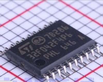
Protected STM32F042F4 Microcontroller Program Recovery
Protected STM32F042F4 Microcontroller Program Recovery starts from crack stm32f042f4 microprocessor’s security fuse bit and extract embedded binary from microcontroller stm32f042f4 flash memory;
The STM32F042x4/x6 microcontrollers incorporate the high-performance
ARM® Cortex®-M0 32-bit RISC core operating at up to 48 MHz frequency, high-speed embedded memories (up to 32 Kbytes of Flash memory and 6 Kbytes of SRAM), and an extensive range of enhanced peripherals and I/Os.
All devices offer standard communication interfaces (one I2C, two SPIs/one I2S, one HDMI CEC and two USARTs), one USB Full-speed device (crystal-less), one CAN, one 12-bit ADC, four 16-bit timers, one 32-bit timer and an advanced-control PWM timer in order to breaking off stm32f038k6 readout protection system.
защищенное восстановление программы микроконтроллера STM32F042F4 начинается с взлома бита предохранителя микропроцессора STM32F042F4 и извлечения встроенного двоичного файла из флэш-памяти микроконтроллера STM32F042F4;
The STM32F042x4/x6 microcontrollers operate in the -40 to +85 °C and -40 to +105 °C temperature ranges, from a 2.0 to 3.6 V power supply. A comprehensive set of power-saving modes allows the design of low-power applications.
Restore ST Microcontroller ST72F32AK2 Encrypted Flash Heximal
Restore ST Microcontroller ST72F32AK2 Encrypted Flash Heximal from embedded flash memory, unlock st72f32ak2 mcu fuse bit protection over its flash memory, then extract heximal file from microprocessor st72f32ak2 locked flash memory;
The ST72F32A and ST7232A devices are mem- bers of the ST7 microcontroller family designed for the 5V operating range.
The 32 and 44-pin devices are designed for mid- range applications All devices are based on a common industry- standard 8-bit core, featuring an enhanced instruc- tion set and are available with FLASH or ROM pro- gram memory.
Under software control, all devices can be placed in WAIT, SLOW, ACTIVE-HALT or HALT mode which can be used for breaking st72f32ak1 mcu flash memory protection;
Reducing power consumption when the application is in idle or stand-by state. The enhanced instruction set and addressing modes of the ST7 offer both power and flexibility to software developers, enabling the design of highly efficient and compact application code.
In addition to standard 8-bit data management, all ST7 micro- controllers feature true bit manipulation, 8×8 un- signed multiplication and indirect addressing modes.
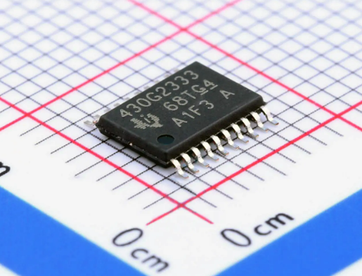
Texas MSP430G2333 Microcontroller Firmware Recovery
Texas MSP430G2333 Microcontroller Firmware Recovery needs to crack ti msp430g2333 microprocessor’s security tamper resistance system, and then extract microprocessor msp430g2333 locked code from its flash memory;

Stresses beyond those listed under “absolute maximum ratings” may cause permanent damage to the device. These are stress ratings only, and functional operation of the device at these or any other conditions beyond those indicated under “recommended operating conditions” is not implied. Exposure to absolute-maximum-rated conditions for extended periods may affect device reliability.
Texas MSP430G2333 mikrodenetleyici ürün yazılımı kurtarma, ti msp430g2333 mikroişlemcinin güvenlik kurcalama direnci sistemini kırmalı ve ardından mikroişlemci msp430g2333 kilitli kodunu flash belleğinden çıkarmalıdır;
All voltages referenced to VSS. The JTAG fuse-blow voltage, VFB, is allowed to exceed the absolute maximum rating. The voltage is applied to the TEST pin when blowing the JTAG fuse which is a common method for cracking msp430g2230 mcu flash memory fuse bit.
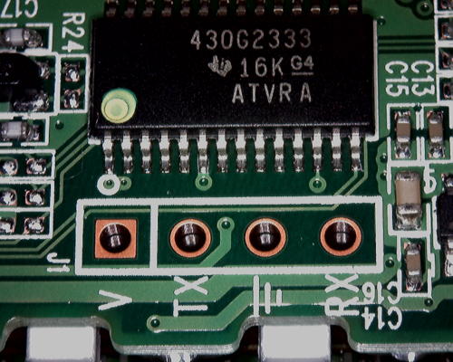
unlock silicon microcontroller MSP430G2333 flash memory and copy heximal program of memory
Higher temperature may be applied during board soldering according to the current JEDEC J-STD-020 specification with peak reflow temperatures not higher than classified on the device label on the shipping boxes or reels.
The MSP430 CPU is clocked directly with MCLK. Both the high and low phase of MCLK must not exceed the pulse duration of the specified maximum frequency when restoring msp430g2001 microcontroller heximal program.
Modules might have a different maximum input clock specification. See the specification of the respective module in this data sheet.
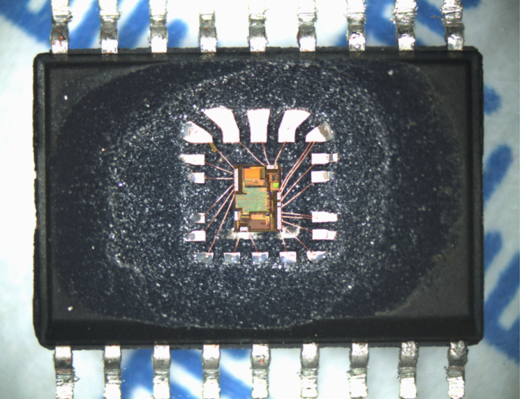
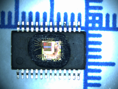
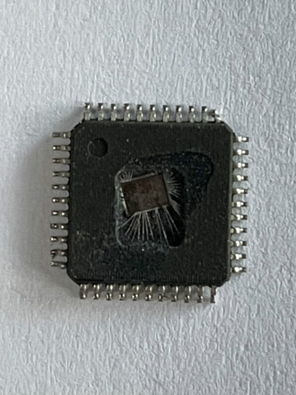
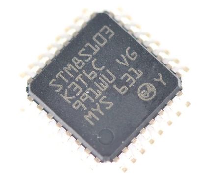
STM8S103K3T6 Microcontroller Embedded Flash Firmware Restoration
STM8S103K3T6 Microcontroller Embedded Flash Firmware Restoration starts from unlock stm8s103k3 security fuse bit by focus ion beam and then extract flash memory code from original stm8s103k3 processor;

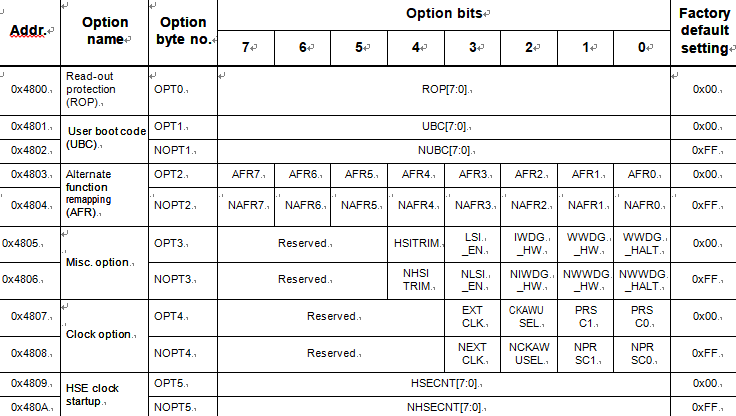
Option bytes contain configurations for device hardware features as well as the memory protection of the device. They are stored in a dedicated block of the memory. Except for the ROP (read-out protection) byte, each option byte has to be stored twice, in a regular form (OPTx) and a complemented one (NOPTx) for redundancy when recover stm8s003k3 memory heximal.
STM8S103K3T6 mikrodenetleyici gömülü flash ürün yazılımı geri yükleme, STM8S103K3 güvenlik sigortasının odak iyon ışını ile bit kilidini açmaktan başlar ve ardından orijinal STM8S103K3 işlemciden flash bellek kodunu çıkarır;
Option bytes can be modified in ICP mode (via SWIM) by accessing the EEPROM address shown in Table 12: Option bytes below. Option bytes can also be modified ‘on the fly’ by the application in IAP mode, except the ROP option that can only be modified in ICP mode (via SWIM).
Refer to the STM8S Flash programming manual (PM0051) and STM8 SWIM communication protocol and debug module user manual (UM0470) for information on SWIM programming procedures in the process of stm8s103k2 mcu flash source code cloning.
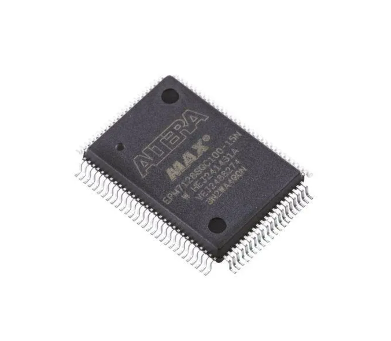
Altera Programmable Logic Device EPM7128BUC169 Firmware Restoration
Altera Programmable Logic Device EPM7128BUC169 Firmware Restoration means the embedded eeprom memory inside original PLD EPM7128BUC processor will be unlocked and firmware can be fully extracted from IC CPLD;
All MAX 7000A devices contain a programmable security bit that controls access to the data programmed into the device. When this bit is programmed, a design implemented in the device cannot be copied or retrieved.
This feature provides a high level of design security because programmed data within EEPROM cells is invisible. The security bit that controls this function, as well as all other programmed data, is reset only when the device is reprogrammed after reverse engineering cpld epm7032aeti44 memory.
Le dispositif logique programmable Altera EPM7128BUC169 la restauration du firmware signifient que la mémoire eeprom intégrée à l’intérieur du processeur PLD EPM7128BUC d’origine sera déverrouillée et que le firmware pourra être entièrement extrait de IC CPLD
MAX 7000A devices are fully tested. Complete testing of each
programmable EEPROM bit and all internal logic elements ensures 100% programming yield. AC test measurements are taken under conditions equivalent to those shown. Test patterns can be used and then erased during early stages of the production flow when recover cpld epm7128 embedded eeprom program.