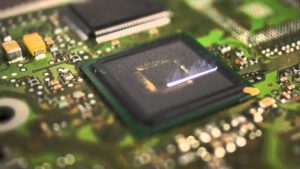
 Break Chip PIC16F59 Eeprom
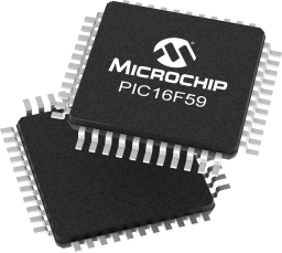
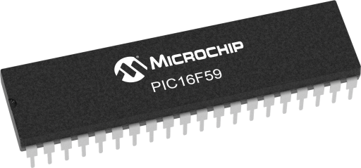
Modern industrial systems rely heavily on stable low-power microcontrollers, and the Microchip PIC16F59 remains a popular choice in manufacturing, appliance control, compact automation modules, and a wide range of embedded designs. As equipment ages, owners often face difficulties accessing the eeprom, flash, and internal memory due to protected, locked, or encrypted configurations. Our high-end service, introduced under the subject Break Chip PIC16F59 EEPROM, is designed to help legitimate clients safely retrieve operational data, program logic, and legacy firmware without exposing any attack techniques.
The high performance of the PIC16F5X family can be attributed to a number of architectural features commonly found in RISC microprocessors to Break Chip PIC16F59 Eeprom. To begin with, the PIC16F5X uses a Harvard architecture in which program and data are accessed on separate buses.
Industry Use Cases & Unique Features of PIC16F59
The PIC16F59 is widely used because of its flexible architecture, low power consumption, and stable embedded design. You will find it in:
- Household electronic controllers
- Industrial signal modules and measurement devices
- Educational hardware, training boards, and simple robotics
- Automotive auxiliary electronics
- Consumer and semi-industrial automation tools
Its internal 12-bit core, versatile I/O structure, and reliable eeprom storage make it a long-term favorite among OEMs. Many manufacturers build custom logic inside this device, making the stored binary or heximal archive extremely valuable to business continuity.
This improves bandwidth over traditional von Neumann architecture where program and data are fetched on the same bus. Separating program and data memory further allows instructions to be sized differently than the 8-bit wide data word. Instruction opcodes are 12-bits wide, making it possible to have all single-word instructions. A 12-bit wide program memory access bus fetches a 12-bit instruction in a single cycle.
A two-stage pipeline overlaps fetch and execution of instructions. Consequently, all instructions (33) execute in a single cycle except for program branches. The PIC16F54 addresses 512 x 12 of program memory, the PIC16F57 and PIC16F59 addresses 2048 x 12 of program memory. All program memory is internal.
The PIC16F5X can directly or indirectly address its register files and data memory. All Special Function Registers (SFR), including the program counter, are mapped in the data memory. The PIC16F5X has a highly orthogonal (symmetrical) instruction set that makes it possible to carry out any operation on any register using any Addressing mode when Break Chip PIC16F59 Eeprom. This symmetrical nature and lack of ‘special optimal situations’ make programming with the PIC16F5X simple, yet efficient. In addition, the learning curve is reduced significantly.
The PIC16F5X device contains an 8-bit ALU and working register. The ALU is a general purpose arithmetic unit. It performs arithmetic and Boolean functions between data in the working register and any register file.
What Our Service Provides
Our service assists authorized device owners who need to break through inaccessible flash or eeprom regions due to forgotten revisions, discontinued suppliers, or lost source code. We support scenarios where systems must continue running for many years, but the original file or firmware is no longer obtainable.
We help legitimate clients:
- Retrieve the internal program and operational data
- Clone or duplicate their existing unit for maintenance or redesign
- Rebuild missing archive records for long-term service
- Recover critical logic damaged by aging components
Although some devices require inspection or controlled decapsulation, we do not disclose any internal processes. The goal is always to return a verified, functional binary or heximal image of your own property.
The ALU is 8-bits wide and capable of addition, subtraction, shift and logical operations. Unless otherwise mentioned, arithmetic operations are two’s complement in nature. In two-operand instructions, typically one operand is the W (working) register. The other operand is either a file register or an immediate constant. In single operand instructions, the operand is either the W register or a file register.
General High-Level Recovery Concept (Non-technical & Safe)
The process begins with a feasibility assessment based on device condition, level of secured configuration, and memory integrity. Some units require physical stabilization or deeper evaluation, while others can be processed through standardized extraction workflows designed to respect IP ownership, legal compliance, and data confidentiality.
Our team does not “teach” customers how to hack, decode, or attack the security. Instead, we perform all procedures internally and return only the final, usable file.
Purpose & Benefits for End Users
Clients choose this service because it helps them:
- Keep old machinery running without redesign
- Preserve unique source code and calibration data
- Extend the life cycle of products reliant on PIC16F59
- Avoid costly downtime caused by lost or inaccessible firmware
- Ensure a secure, company-controlled archive for future engineering
By providing a complete and validated memory image, we enable stable maintenance, redesign, or modernization.
Typical Challenges We Encounter
Recovery of PIC16F59 may involve:
- Heavily protected or embedded firmware regions
- Partial memory decay or corruption
- Environmental wear or physical damage
- Complex security configurations depending on revision
Despite these difficulties, our methodical workflow and advanced evaluation tools help ensure high success rates under legally authorized conditions.
The W register is an 8-bit working register used for ALU operations. It is not an addressable register. Depending on the instruction executed, the ALU may affect the values of the Carry (C), Digit Carry (DC) and Zero (Z) bits in the STATUS Register to Extract IC code. The C and DC bits operate as a borrow and digit borrow out bit, respectively, in subtraction. See the SUBWF and ADDWF instructions for examples.
A simplified block diagram is shown in Figure 2-1 with the corresponding device pins described in Table 2-1 (for PIC16F54), Table 2-2 (for PIC16F57) and Table 2-3 (for PIC16F59).