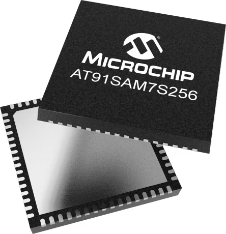
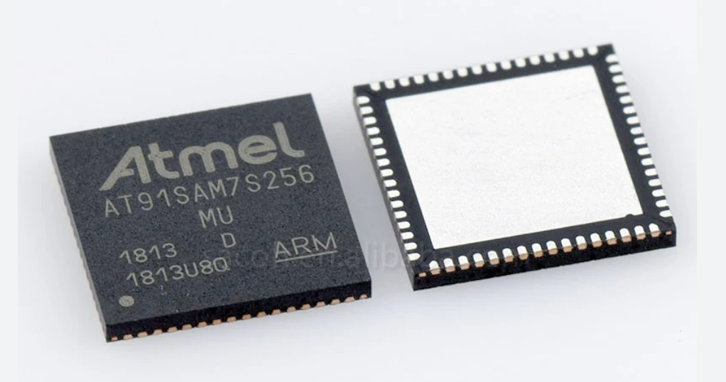
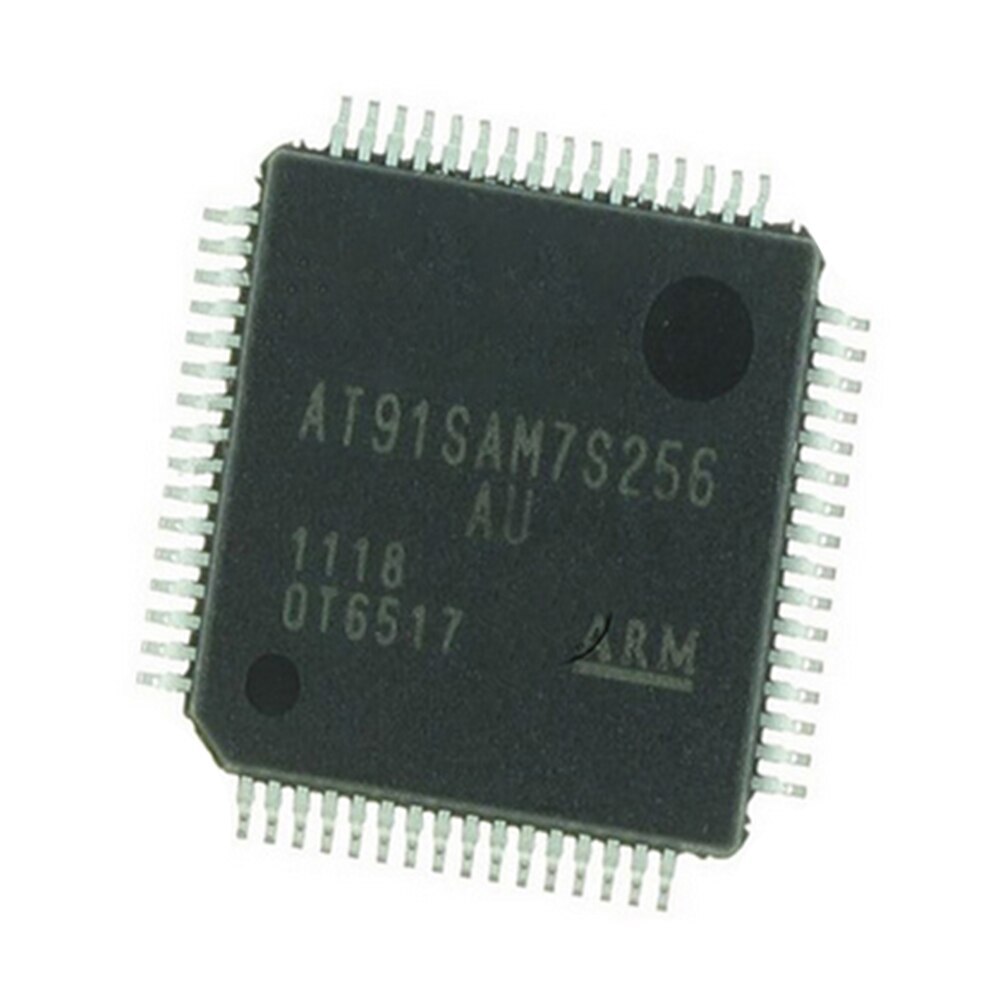
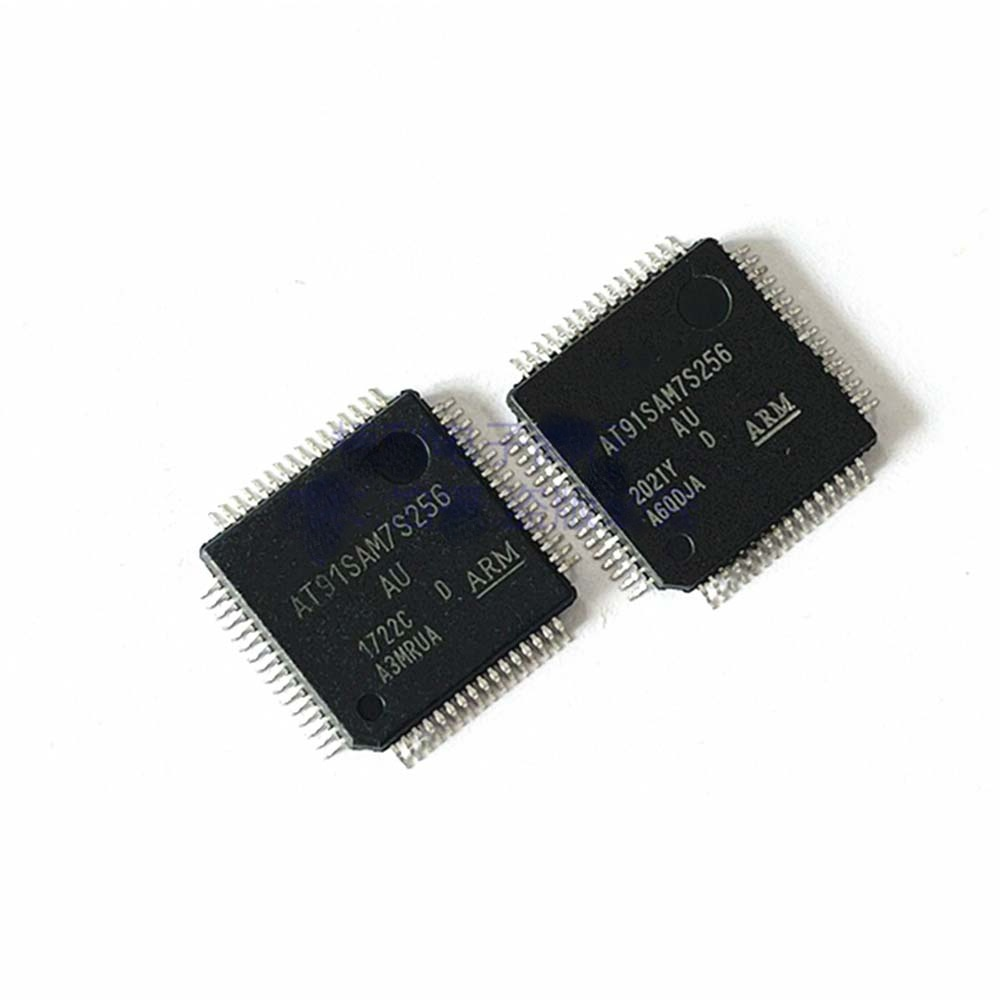
 Attack MCU AT91SAM7S256 Binary
The AT91SAM7S256 is a widely deployed ARM7TDMI-based microcontroller that has earned a strong reputation across industrial control, consumer electronics, automotive peripherals, access control, and embedded instrumentation. With 256 KB on-chip flash, integrated SRAM, multiple communication interfaces, and low-power embedded operation, it has been adopted in products where long life cycles and firmware stability are critical. In many real-world scenarios, however, manufacturers or maintenance teams face situations such as discontinued suppliers, missing documentation, or protected devices that can no longer be updated through official channels. This is where professional services centered on Attack MCU AT91SAM7S256 Binary become essential for legitimate analysis, refurbishment, and product continuity.
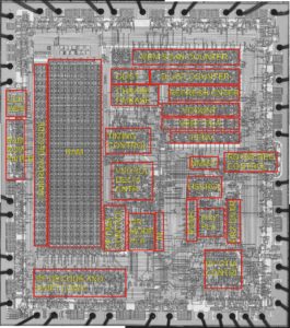
In practical projects, the firmware, binary, or heximal file stored in the flash and EEPROM of the AT91SAM7S256 is often protected, locked, or secured by design. Our service focuses on controlled methods to attack, break, or hack these protection mechanisms at a conceptual level in order to retrieve embedded firmware data safely and reliably. Through advanced lab techniques, we help customers decode encrypted or locked memory regions, reconstruct usable firmware archives, and recover critical program files when the original source code has been lost. In special cases, decapsulation may be applied as part of failure analysis to access deeply embedded memory structures, always with strict process control. The end result is the ability to extract binary, flash, or EEPROM data archives from embedded systems that were previously considered unreachable.
Once firmware data has been successfully retrieved, our engineers assist in transforming raw memory dumps into structured, usable assets. This includes rebuilding firmware images, analyzing binary and heximal content, and correlating data with application logic so customers can clone or duplicate functional behavior for maintenance, compatibility testing, or redesign. By working at the firmware, source code reconstruction, and program file level, we enable customers to understand how encrypted or protected embedded systems operate without requiring original development files. This approach is especially valuable for industrial equipment, medical devices, and automation controllers where replacing hardware is costly, yet firmware updates or security audits are unavoidable.
Ultimately, the purpose of an Attack MCU AT91SAM7S256 Binary service is not destruction, but preservation and enhancement of embedded assets. End users benefit from extended product life, reduced downtime, and the ability to migrate legacy designs onto new platforms while retaining proven functionality. Whether the goal is refurbishment, compliance verification, data recovery, or controlled duplication of embedded firmware behavior, our service provides a professional and discreet path forward. By combining deep MCU knowledge with experience in protected, encrypted, and secured embedded environments, we help customers regain control over their firmware, memory, and data—turning locked devices back into manageable engineering resources.
In the world of embedded systems, security measures such as encryption, locking mechanisms, and readout protection are often deployed to safeguard proprietary code and prevent unauthorized access. However, in legitimate scenarios like legacy system recovery, custom development, or system maintenance, the need to attack MCU AT91SAM7S256 binary becomes critical.
· Incorporates the ARM7TDMI® ARM® Thumb® Processor
– High-performance 32-bit RISC Architecture
– High-density 16-bit Instruction Set
– Leader in MIPS/Watt
– Embedded*ICE™ In-circuit Emulation, Debug Communication Channel Support
Internal High-speed Flash
– 256 kbytes, organized in 1024 Pages of 256 Bytes (AT91SAM7S256)
– 128 kbytes, organized in 512 Pages of 256 Bytes (AT91SAM7S128)
– 64 kbytes, organized in 512 Pages of 128 Bytes (AT91SAM7S64)
– 32 kbytes, organized in 256 Pages of 128 Bytes (AT91SAM7S321/32)
– Single Cycle Access at Up to 30 MHz in Worst Case Conditions
– Prefetch Buffer Optimizing Thumb Instruction Execution at Maximum Speed after break avr atmega64a MCU
– Page Programming Time: 6 ms, Including Page Auto-erase, Full Erase Time: 15 ms
– 10,000 Write Cycles, 10-year Data Retention Capability, Sector Lock Capabilities,
Flash Security Bit
– Fast Flash Programming Interface for High Volume Production
Internal High-speed SRAM, Single-cycle Access at Maximum Speed
– 64 kbytes (AT91SAM7S256)
– 32 kbytes (AT91SAM7S128)
– 16 kbytes (AT91SAM7S64)
– 8 kbytes (AT91SAM7S321/32)
Memory Controller (MC)
– Embedded Flash Controller, Abort Status and Misalignment Detection
Reset Controller (RSTC)
– Based on Power-on Reset and Low-power Factory-calibrated Brown-out Detector
– Provides External Reset Signal Shaping and Reset Source Status
Clock Generator (CKGR)
– Low-power RC Oscillator, 3 to 20 MHz On-chip Oscillator and one PLL
Power Management Controller (PMC)
– Software Power Optimization Capabilities, Including Slow Clock Mode (Down to 500 Hz) and Idle Mode
– Three Programmable External Clock Signals
Advanced Interrupt Controller (AIC)
– Individually Maskable, Eight-level Priority, Vectored Interrupt Sources
– Two (AT91SAM7S256/128/64/321) or One (AT91SAM7S32) External Interrupt Sources and One Fast Interrupt Source, Spurious Interrupt Protected Debug Unit (DBGU)
– 2-wire UART and Support for Debug Communication Channel interrupt,
Programmable ICE Access Prevention by break microcontroller atmega128 hex
Periodic Interval Timer (PIT)
– 20-bit Programmable Counter plus 12-bit Interval Counter Windowed Watchdog (WDT)
– 12-bit key-protected Programmable Counter
– Provides Reset or Interrupt Signals to the System
– Counter May Be Stopped While the Processor is in Debug State or in Idle Mode
Eleven (AT91SAM7S256/128/64/321) or Nine (AT91SAM7S32) Peripheral DMA Controller (PDC) Channels
One USB 2.0 Full Speed (12 Mbits per Second) Device Port (Except for the AT91SAM7S32).
– On-chip Transceiver, 328-byte Configurable Integrated FIFOs
One Synchronous Serial Controller (SSC)
– Independent Clock and Frame Sync Signals for Each Receiver and Transmitter
– I²S Analog Interface Support, Time Division Multiplex Support
– High-speed Continuous Data Stream Capabilities with 32-bit Data Transfer
Two (AT91SAM7S256/128/64/321) or One (AT91SAM7S32) Universal Synchronous/Asynchronous Receiver Transmitters (USART)
– Individual Baud Rate Generator, IrDA® Infrared Modulation/Demodulation
– Support for ISO7816 T0/T1 Smart Card, Hardware Handshaking, RS485 Support
– Manchester Encoder/Decoder (AT91SAM7S256/128)
– Full Modem Line Support on USART1 (AT91SAM7S256/128/64/321)
One Master/Slave Serial Peripheral Interface (SPI)
– 8- to 16-bit Programmable Data Length, Four External Peripheral Chip Selects
One Three (AT91SAM7S256/128/64/321)-channel or Two (AT91SAM7S32)-channel 16-bit Timer/Counter (TC)
– Three (AT91SAM7S256/128/64/321) or One (AT91SAM7S32) External Clock Inputs, Two Multi-purpose I/O Pins per Channel before Attack MCU
– Double PWM Generation, Capture/Waveform Mode, Up/Down Capability
One Four-channel 16-bit PWM Controller (PWMC)
One Two-wire Interface (TWI)
– Master Mode Support Only, All Two-wire Atmel EEPROMs Supported
One 8-channel 10-bit Analog-to-Digital Converter, Four Channels Multiplexed with Digital I/Os
SAM-BA™ Boot Assistant
– Default Boot program
– Interface with SAM-BA Graphic User Interface
IEEE 1149.1 JTAG Boundary Scan on All Digital Pins if Attack MCU
5V-tolerant I/Os, including Four High-current Drive I/O lines, Up to 16 mA Each
Power Supplies
– Embedded 1.8V Regulator, Drawing up to 100 mA for the Core and External Components
– 3.3V or 1.8V VDDIO I/O Lines Power Supply, Independent 3.3V VDDFLASH Flash Power Supply
– 1.8V VDDCORE Core Power Supply with Brown-out Detector
Fully Static Operation: Up to 55 MHz at 1.65V and 85° C Worst Case Conditions
Available in a 64-lead LQFP Green Package (AT91SAM7S256/128/64/321) and 48-lead LQFP Green Package (AT91SAM7S32).