Archive for May, 2014
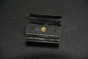
 Copy Microcontroller AT89C51RE2 Binary
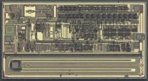
Copy Microcontroller AT89C51RE2 Binary
Copy Microcontroller AT89C51RE2 Binary from its flash and eeprom memory, then replicate the program and data to other blank MCU AT89C51RE2 for the same functions;
· 80C52 Compatible
– 8051 Instruction Compatible
– Four 8-bit I/O Ports (44 Pins Version)
– Three 16-bit Timer/Counters
– 256 bytes Scratch Pad RAM
– 11 Interrupt Sources With 4 Priority Levels if Copy Microcontroller
ISP (In-System Programming) Using Standard VCC Power Supply
Integrated Power Monitor (POR/PFD) to Supervise Internal Power Supply
Boot ROM Contains Serial Loader for In-System Programming
High-speed Architecture after Copy Microcontroller
– In Standard Mode:
40 MHz (Vcc 2.7V to 5.5V, Both Internal and External Code Execution)
60 MHz (Vcc 4.5V to 5.5V and Internal Code Execution Only)
– In X2 Mode (6 Clocks/Machine Cycle)
20 MHz (Vcc 2.7V to 5.5V, Both Internal and External Code Execution)
30 MHz (Vcc 4.5V to 5.5V and Internal Code Execution Only)
128K bytes On-chip Flash Program/Data Memory
– 128 bytes Page Write with auto-erase when Copy Microcontroller
– 100k Write Cycles
On-chip 8192 bytes Expanded RAM (XRAM)
– Software Selectable Size (0, 256, 512, 768, 1024, 1792, 2048, 4096, 8192 bytes)
Extended stack pointer to 512 bytes
Variable Length MOVX for Slow RAM/Peripherals
Improved X2 Mode with Independant Selection for CPU and Each Peripheral
Keyboard Interrupt Interface on Port 1
SPI Interface (Master/Slave Mode) after Copy Microcontroller
8-bit Clock Prescaler
Programmable Counter Array with:
– High Speed Output
– Compare/Capture
– Watchdog Timer Capabilities
Asynchronous Port Reset
Two Full Duplex Enhanced UART with Dedicated Internal Baud Rate Generator
Low EMI (inhibit ALE)
Hardware Watchdog Timer (One-time Enabled with Reset-Out), Power-Off Flag
Power Control Modes: Idle Mode, Power-down Mode
Power Supply: 2.7V to 5.5V when Copy Microcontroller
Temperature Ranges: Industrial (-40 to +85°C)
Packages: PLCC44, VQFP44
Attack Microcontroller W77E058A40DL Flash
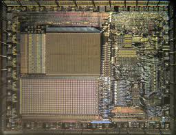
Attack Microcontroller W77E058A40DL Flash
Attack Microcontroller W77E058A40DL Flash memory and disable the protective mechanism on it, extract firmware out from the MCU;
FEATURES
8-bit CMOS microcontroller
High speed architecture of 4 clocks/machine cycle runs up to 40 MHz
Pin compatible with standard 80C52
Instruction-set compatible with MCS-51
Four 8-bit I/O Ports
One extra 4-bit I/O port and Wait State control signal (available on 44-pin PLCC/QFP package)
Three 16-bit Timers when Attack Microcontroller
12 interrupt sources with two levels of priority
On-chip oscillator and clock circuitry
Two enhanced full duplex serial ports
32 KB Flash EPROM
256 bytes scratch-pad RAM
1 KB on-chip SRAM for MOVX instruction
Programmable Watchdog Timer
Dual 16-bit Data Pointers after Attack Microcontroller
Software programmable access cycle to external RAM/peripherals
Packages:
− Lead Free(RoHS) DIP 40:
W77E058A40DL
− Lead Free(RoHS) PLCC 44: W77E058A40PL
− Lead Free(RoHS) PQFP 44: W77E058A40FL if Attack Microcontroller
GENERAL DESCRIPTION
The W77E058 is a fast 8051 compatible microcontroller with a redesigned processor core without
wasted clock and memory cycles. As a result, it executes every 8051 instruction faster than the
original 8051 for the same crystal speed. Typically, the instruction executing time of W77E058 is 1.5 to 3 times faster then that of traditional 8051, depending on the type of instruction when Attack Microcontroller. In general, the overall performance is about 2.5 times better than the original for the same crystal speed. Giving the same throughput with lower clock speed, power consumption has been improved. Consequently, the W77E058 is a fully static CMOS design; it can also be operated at a lower crystal clock. The W77E058 contains 32 KB Flash EPROM, and provides operating voltage from 4.5V to 5.5V before Attack Microcontroller. All W77E058 types also support on-chip 1 KB SRAM without external memory component and glue logic, saving more I/O pins for users’ application usage if they use on-chip SRAM instead of external SRAM.
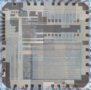
Attack MCU ATmega162 Flash

Attack MCU ATmega162 can help engineer to find out the location of security fuse bit then use laser cutting to remove it, and reset the status of Microcontroller from locked to unlocked;
Features
· High-performance, Low-power AVR® 8-bit Microcontroller
· Advanced RISC Architecture
– 131 Powerful Instructions – Most Single-clock Cycle Execution
– 32 x 8 General Purpose Working Registers
– Fully Static Operation
– Up to 16 MIPS Throughput at 16 MHz when Attack MCU
– On-chip 2-cycle Multiplier
Non-volatile Program and Data Memories
– 16K Bytes of In-System Self-programmable Flash Endurance: 10,000 Write/Erase Cycles
– Optional Boot Code Section with Independent Lock Bits
In-System Programming by On-chip Boot Program
True Read-While-Write Operation
– 512 Bytes EEPROM
Endurance: 100,000 Write/Erase Cycles
– 1K Bytes Internal SRAM
– Up to 64K Bytes Optional External Memory Space after Attack MCU
8-bit
Microcontroller
with 16K Bytes
In-System
– Programming Lock for Software Security
JTAG (IEEE std. 1149.1 Compliant) Interface
– Boundary-scan Capabilities According to the JTAG Standard
– Extensive On-chip Debug Support before Attack MCU
– Programming of Flash, EEPROM, Fuses, and Lock Bits through the JTAG Interface
Peripheral Features
– Two 8-bit Timer/Counters with Separate Prescalers and Compare Modes
– Two 16-bit Timer/Counters with Separate Prescalers, Compare Modes, and
Capture Modes
– Real Time Counter with Separate Oscillator
– Six PWM Channels
– Dual Programmable Serial USARTs if Attack MCU
– Master/Slave SPI Serial Interface
– Programmable Watchdog Timer with Separate On-chip Oscillator
– On-chip Analog Comparator
Special Microcontroller Features
– Power-on Reset and Programmable Brown-out Detection
– Internal Calibrated RC Oscillator
– External and Internal Interrupt Sources after Attack MCU
– Five Sleep Modes: Idle, Power-save, Power-down, Standby, and Extended Standby
I/O and Packages
– 35 Programmable I/O Lines
– 40-pin PDIP, 44-lead TQFP, and 44-pad MLF
Operating Voltages
– 1.8 – 5.5V for ATmega162V
– 2.7 – 5.5V for ATmega162
Speed Grades
Programmable Flash
ATmega162
ATmega162V if Attack MCU
– 0 – 8 MHz for ATmega162V (see Figure 113 on page 265)
– 0 – 16 MHz for ATmega162 (see Figure 114 on page 265)
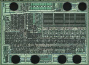
Attack Chip PIC16F72 Heximal
Attack Chip PIC16F72 and extract content from memory out then copy the code to other blank microcontroller PIC16F72, the format of code will be Heximal;
Devices Included In This Data Sheet:
Low-Power Features:
· Standby Current:
– 40 nA @ 1.8V, typical
· Operating Current:
High-Performance RISC CPU when Attack Chip:
· Only 35 Instructions to Learn:
– All single-cycle instructions except branches
· Operating Speed:
– DC – 16 MHz oscillator/clock input
– DC – 250 ns instruction cycle
· Up to 4K x 14 Words of Flash Program Memory
· Up to 256 bytes of Data Memory (RAM)
· Interrupt Capability
· 8-Level Deep Hardware Stack
· Direct, Indirect and Relative Addressing modes if Attack Chip
· Processor Self-Write/Read access to Program Memory
Special Microcontroller Features:
· Precision Internal Oscillator:
– 16 MHz or 500 kHz operation
– Factory calibrated to ±1%, typical
– Software tunable
– Software selectable ÷1, ÷2, ÷4 or ÷8 divider
· Power-Saving Sleep mode
· Industrial and Extended Temperature Range before Attack Chip
· Power-on Reset (POR)
· Power-up Timer (PWRT)
· Brown-out Reset (BOR)
· Multiplexed Master Clear with Pull-up/Input Pin
· Programmable Code Protection
· In-Circuit Serial ProgrammingTM (ICSPTM) via Two Pins
· 128 Bytes High-Endurance Flash:
– 100,000 write Flash endurance (minimum) after Attack Chip
· Wide Operating Voltage Range:
– 1.8V to 5.5V (PIC16F720/721)
– 1.8V to 3.6V (PIC16LF720/721)
– 35 mA/MHz @ 1.8V, typical
· Low-Power Watchdog Timer Current:
– 500 nA @ 1.8V, typical
Peripheral Features:
· Up to 17 I/O Pins and 1 Input-only Pin:
– High-current source/sink for direct LED drive after Attack Chip
– Interrupt-on-change pins
– Individually programmable weak pull-ups
· A/D Converter:
– 8-bit resolution
– 12 channels
– Selectable Voltage reference
· Timer0: 8-Bit Timer/Counter with 8-Bit Programmable Prescaler
· Enhanced Timer1
– 16-bit timer/counter with prescaler
– External Gate Input mode with toggle and single shot modes for Attack Chip
– Interrupt-on-gate completion
· Timer2: 8-Bit Timer/Counter with 8-Bit Period Register, Prescaler and Postscaler
· Capture, Compare, PWM module (CCP)
– 16-bit Capture, max resolution 12.5 ns
– 16-bit Compare, max resolution 250 ns
– 10-bit PWM, max frequency 15 kHz
· Addressable Universal Synchronous
Asynchronous Receiver Transmitter (AUSART)
· Synchronous Serial Port (SSP)
– SPI (Master/Slave)
– I2CTM (Slave) with Address Mask when Attack Chip
Copy MCU AT89C55WD Binary
Copy MCU AT89C55WD Binary means the firmware from both eeprom and flash will be readout and rewrite to other blank Microcontroller AT89C55WD which will provide the same functions as originals;
Compatible with MCS®-51 Products
20K Bytes of Reprogrammable Flash Memory
Endurance: 10,000 Write/Erase Cycles
4V to 5.5V Operating Range when Copy MCU
Fully Static Operation: 0 Hz to 33 MHz
Three-level Program Memory Lock
256 x 8-bit Internal RAM
32 Programmable I/O Lines
Three 16-bit Timer/Counters after Copy MCU
Eight Interrupt Sources
Programmable Serial Channel
Low-power Idle and Power-down Modes
Interrupt Recovery from Power-down Mode
Hardware Watchdog Timer if Copy MCU
Dual Data Pointer
Power-off Flag
Green (Pb/Halide-free) Packaging Option before Copy MCU
Circuit Engineering Company Limited continues to be recognized as the Southern China Leader in Services for IC Break, MCU attack, Chip Recover, Microcontroller Copy service. With the advancement of today’s modern circuit board technology, it is more important than ever to have specialists available to help you at a moment’s notice. Our engineering and commercial teams collectively have a vast amount of electronic experience covering field include Consumer Electronics, Industrial Automation Electronics, Wireless Communication Electronics., etc. For more information please contact us through email.
Copy IC PIC16F886 Firmware
Copy IC PIC16F886 Firmware and reprogramme the program into blank Microcontroller PIC16F886 which will provide the same functions as original MCU PIC16F886 after Crack MCU protective system;
Copy IC PIC16F886 Firmware and reprogramme the program into blank Microcontroller PIC16F886 which will provide the same functions as original MCU PIC16F886 after Crack MCU protective system
High-Performance RISC CPU:
· Only 35 instructions to learn:
– All single-cycle instructions except branches
· Operating speed:
– DC – 20 MHz oscillator/clock input
– DC – 200 ns instruction cycle
· Interrupt capability
· 8-level deep hardware stack
· Direct, Indirect and Relative Addressing modes
Special Microcontroller Features:
· Precision Internal Oscillator:
– Factory calibrated to ±1%
– Software selectable frequency range of 8 MHz to 31 kHz
– Software tunable
– Two-Speed Start-up mode
– Crystal fail detect for critical applications
– Clock mode switching during operation for power savings
· Power-Saving Sleep mode
· Wide operating voltage range (2.0V-5.5V)
· Industrial and Extended Temperature range
· Power-on Reset (POR)
· Power-up Timer (PWRT) and Oscillator Start-up Timer (OST)
· Brown-out Reset (BOR) with software control option
· Enhanced low-current Watchdog Timer (WDT) with on-chip oscillator (software selectable nominal 268 seconds with full prescaler) with software enable
· Multiplexed Master Clear with pull-up/input pin
· Programmable code protection
· High Endurance Flash/EEPROM cell:
– 100,000 write Flash endurance
– 1,000,000 write EEPROM endurance
– Flash/Data EEPROM retention: > 40 years
· Program memory Read/Write during run time
· In-Circuit Debugger (on board)
Low-Power Features:
· Standby Current:
– 50 nA @ 2.0V, typical
· Operating Current:
– 11 ìA @ 32 kHz, 2.0V, typical
– 220 ìA @ 4 MHz, 2.0V, typical
· Watchdog Timer Current:
– 1 ìA @ 2.0V, typical
Peripheral Features:
· 24/35 I/O pins with individual direction control
– High current source/sink for direct LED drive
– Interrupt-on-Change pin
– Individually programmable weak pull-ups
– Ultra Low-Power Wake-up (ULPWU)
· Analog Comparator module with:
– Two analog comparators
– Programmable on-chip voltage reference (CVREF) module (% of VDD)
– Fixed voltage reference (0.6V)
– Comparator inputs and outputs externally accessible
– SR Latch mode
– External Timer1 Gate (count enable)
· A/D Converter:
– 10-bit resolution and 11/14 channels
· Timer0: 8-bit timer/counter with 8-bit programmable prescaler
· Enhanced Timer1:
– 16-bit timer/counter with prescaler
– External Gate Input mode
– Dedicated low-power 32 kHz oscillator
· Timer2: 8-bit timer/counter with 8-bit period register, prescaler and postscaler
· Enhanced Capture, Compare, PWM+ module:
– 16-bit Capture, max. resolution 12.5 ns
– Compare, max. resolution 200 ns
– 10-bit PWM with 1, 2 or 4 output channels, programmable “dead time”, max. frequency 20 kHz
– PWM output steering control
· Capture, Compare, PWM module:
– 16-bit Capture, max. resolution 12.5 ns
– 16-bit Compare, max. resolution 200 ns
– 10-bit PWM, max. frequency 20 kHz
· Enhanced USART module:
– Supports RS-485, RS-232, and LIN 2.0
– Auto-Baud Detect
– Auto-Wake-Up on Start bit
· In-Circuit Serial ProgrammingTM (ICSPTM) via two pins
· Master Synchronous Serial Port (MSSP) module supporting 3-wire SPI (all 4 modes) and I2C™ Master and Slave Modes with I2C address mask
Attack IC MB90F598 Firmware
We can Break IC MB90F598 Firmware, please view the IC MB90F598 features below for your reference:
The MB90595/595G series with FULL-CAN*1 interface and FLASH ROM is especially designed for automotive and industrial applications. Its main features are two on board CAN Interfaces, which conform to V2.0 Part A and Part B, while supporting a very flexible message buffer scheme and so offering more functions than a normal full CAN approach when Attack IC.
The instruction set of F2MC-16LX CPU core inherits an AT architecture of the F2MC*2 family with additional instruction sets for high-level languages, extended addressing mode, enhanced multiplication/division instructions, and enhanced bit manipulation instructions. The microcontroller has a 32-bit accumulator for processing long word data after Attack IC.
The MB90595/595G series has peripheral resources of 8/10-bit A/D converters, UART (SCI), extended I/O serial interface, 8/16-bit PPG timer, I/O timer (input capture (ICU), output compare (OCU)) and stepping motor controller if Attack IC.
*1: Controller Area Network (CAN) – License of Robert Bosch GmbH
*2: F2MC stands for FUJITSU Flexible Microcontroller.
Clock
Embedded PLL clock multiplication circuit
Operating clock (PLL clock) can be selected from divided-by-2 of oscillation or one to four times the oscillation (at oscillation of 4 MHz, 4 MHz to 16 MHz) before Attack IC.
Minimum instruction execution time: 62.5 ns (operation at oscillation of 4 MHz, four times the oscillation clock, VCC of 5.0 V)
Instruction set to optimize controller applications
Rich data types (bit, byte, word, long word)
Rich addressing mode (23 types)
Enhanced signed multiplication/division instruction and RETI instruction functions after Attack IC
Enhanced precision calculation realized by the 32-bit accumulator
· Instruction set designed for high level language (C language) and multi-task operations
Adoption of system stack pointer
Enhanced pointer indirect instructions
Barrel shift instructions
· Program patch function (for two address pointers)
· Enhanced execution speed: 4-byte instruction queue
· Enhanced interrupt function: 8 levels, 34 factors when Attack IC
· Automatic data transmission function independent of CPU operation
Extended intelligent I/O service function (EI2OS): Up to 10 channels
· Embedded ROM size and types
Mask ROM: 128 Kbytes
Flash ROM: 128 Kbytes
Embedded RAM size: 4 Kbytes (MB90V595/595G : 6 Kbytes)
· Flash ROM
Supports automatic programming, Embedded Algorithm TM*
Write/Erase/Erase-Suspend/Resume commands after Attack IC
A flag indicating completion of the algorithm
Hard-wired reset vector available in order to point to a fixed boot sector
Erase can be performed on each block
Block protection with external programming voltage
· Low-power consumption (stand-by) mode
Sleep mode (mode in which CPU operating clock is stopped)
Stop mode (mode in which oscillation is stopped)
CPU intermittent operation mode
Hardware stand-by mode
· Process: 0.5 µm CMOS technology
· I/O port
General-purpose I/O ports: 78 ports
Push-pull output and Schmitt trigger input.
Programmable on each bit as I/O or signal for peripherals for Attack IC.
· Timer
Watchdog timer: 1 channel
8/16-bit PPG timer: 8/16-bit × 6 channels
16-bit re-load timer: 2 channels
· 16-bit I/O timer
Input capture: 4 channels
Output compare: 4 channels
· Extended I/O serial interface: 1 channel
· UART0
With full-duplex double buffer (8-bit length)
Clock asynchronized or clock synchronized (with start/stop bit) transmission can be selectively used.
UART1 (SCI)
With full-duplex double buffer (8-bit length)
Clock asynchronized or clock synchronized serial transmission (I/O extended transmission) can be selectively used if Attack IC.
· Stepping motor controller (4 channels)
· External interrupt circuit (8 channels)
A module for starting an extended intelligent I/O service (EI2OS) and generating an external interrupt which is triggered by an external input.
· Delayed interrupt generation module: Generates an interrupt request for switching tasks.
· 8/10-bit A/D converter (8 channels)
8/10-bit resolution can be selectively used.
Starting by an external trigger input.
· FULL-CAN interface: 1 channel
Conforming to Version 2.0 Part A and Part B
Flexible message buffering (mailbox and FIFO buffering can be mixed) after Attack IC
· 18-bit Time-base counter
· External bus interface: Maximum address space 16 Mbytes
*: Embedded Algorithm is a trademark of Advanced Micro Devices Inc.
Break Chip PIC16F716 Heximal
Break Chip PIC16F716 and extract Heximal out from MCU PIC16F716 flash memory, the security fuse bit of Microcontroller PIC16F716 can be removed or disable for the original MCU PIC16F716
Break Chip PIC16F716 and extract Heximal out from MCU PIC16F716 flash memory, the security fuse bit of Microcontroller PIC16F716 can be removed or disable for the original MCU PIC16F716;
Microcontroller Core Features:
· High-performance RISC CPU
· Only 35 single-word instructions to learn
– All single-cycle instructions except for
program branches which are two-cycle
· Operating speed: DC – 20 MHz clock input
DC – 200 ns instruction cycle
· Interrupt capability (up to 7 internal/external interrupt sources)
· 8-level deep hardware stack
· Direct, Indirect and Relative Addressing modes
Special Microcontroller Features:
· Power-on Reset (POR)
· Power-up Timer (PWRT) and
Oscillator Start-up Timer (OST)
· Watchdog Timer (WDT) with its own on-chip RC
oscillator for reliable operation
· Dual level Brown-out Reset circuitry
– 2.5 VBOR (Typical)
– 4.0 VBOR (Typical)
· Programmable code protection
· Power-Saving Sleep mode
· Selectable oscillator options
· Fully static design
· In-Circuit Serial Programming (ICSP™)
CMOS Technology:
· Wide operating voltage range:
– Industrial: 2.0V to 5.5V
– Extended: 3.0V to 5.5V
· High Sink/Source Current 25/25 mA
· Wide temperature range:
– Industrial: -40°C to 85°C
– Extended: -40°C to 125°C
Low-Power Features:
· Standby Current:
– 100 nA @ 2.0V, typical
· Operating Current:
– 14 ìA @ 32 kHz, 2.0V, typical
– 120 ìA @ 1 MHz, 2.0V, typical
– 1 ìA @ 2.0V, typical
· Timer1 Oscillator Current:
– 3.0 ìA @ 32 kHz, 2.0V, typical
Peripheral Features:
· Timer0: 8-bit timer/counter with 8-bit prescaler can be incremented during Sleep via external crystal/clock
· Timer2: 8-bit timer/counter with 8-bit period register, prescaler and postscaler
· Enhanced Capture, Compare, PWM module:
– Capture is 16-bit, max. resolution is 12.5 ns
– Compare is 16-bit, max. resolution is 200 ns
– PWM maximum resolution is 10-bit
– Enhanced PWM:
– Single, Half-Bridge and Full-Bridge modes
– Digitally programmable dead-band delay
– Auto-shutdown/restart
· 8-bit multi-channel Analog-to-Digital Converter
· 13 I/O pins with individual direction control
· Programmable weak pull-ups on PORTB
Break Microcontroller MC68376BACAB25 Program
We can Break Microcontroller MC68376BACAB25 Program, please view below Microcontroller MC68376BACAB25 features for your reference:
The MC68336 and the MC68376 are highly-integrated 32-bit microcontrollers, combining high-performance data manipulation capabilities with powerful peripheral subsystems.
MC68300 microcontrollers are built up from standard modules that interface through a common intermodule bus (IMB). Standardization facilitates rapid development of devices tailored for specific applications when Break Microcontroller.
The MC68336 incorporates a 32-bit CPU (CPU32), a system integration module (SIM), a time processor unit (TPU), a configurable timer module (CTM4), a queued serial module (QSM), a 10-bit queued analog-to-digital converter module (QADC), a 3.5-Kbyte TPU emulation RAM module (TPURAM), and a 4-Kbyte standby RAM module (SRAM) if Break Microcontroller.
The MC68376 includes all of the aforementioned modules, plus a CAN 2.0B protocol controller module (TouCAN™) and an 8-Kbyte masked ROM (MRM).
The MC68336/376 can either synthesize the system clock signal from a fast reference or use an external clock input directly after Break Microcontroller. Operation with a 4.194 MHz reference frequency is standard. The maximum system clock speed is 20.97 MHz. System hardware and software allow changes in clock rate during operation. Because MCU operation is fully static, register and memory contents are not affected by clock rate changes before Break Microcontroller.
High-density complementary metal-oxide semiconductor (HCMOS) architecture makes the basic power consumption of the MCU low. Power consumption can be minimized by stopping the system clock. The CPU32 instruction set includes a low-power stop (LPSTOP) instruction that efficiently implements this capability after Break Microcontroller.
Documentation for the Modular Microcontroller Family follows the modular construction of the devices in the product line. Each microcontroller has a comprehensive user’s manual that provides sufficient information for normal operation of the device before Break Microcontroller.
The user’s manual is supplemented by module reference manuals that provide detailed information about module operation and applications. Refer to Motorola publication Advanced Microcontroller Unit (AMCU) Literature (BR1116/D) for a complete listing of documentation when Break IC.
Break MCU MC68HC11F1CFN3 Heximal
Break MCU MC68HC11F1CFN3 tamper resistance system and read heximal file out from Microcontroller MC68HC11F1, status of Microprocessor will be reset from locked to unlocked one
Break MCU MC68HC11F1CFN3 tamper resistance system and read heximal file out from Microcontroller MC68HC11F1, status of Microprocessor will be reset from locked to unlocked one;
Features
· MC68HC11 CPU
· Power Saving STOP and WAIT Modes
· 4 Kbytes of On-Chip ROM
· 192 Bytes of On-Chip RAM (All Saved During Standby)
· 16-Bit Timer System
— 3 Input Capture (IC) Channels
— 4 Output Compare (OC) Channels
— One IC or OC Channel (Software Selectable)
· 8-Bit Pulse Accumulator
· Real-Time Interrupt Circuit
· Computer Operating Properly (COP) Watchdog System
· Synchronous Serial Peripheral Interface (SPI)
· Asynchronous Nonreturn to Zero (NRZ) Serial Communications Interface (SCI)
· 26 Input/Output (I/O) Pins
— 16 Bidirectional I/O Pins
— 3 Input Only Pins
— 3 Output Only Pins (One Output Only Pin in the 40-Pin Package)
· Available in a 44-Pin Plastic Leaded Chip Carrier (PLCC) and 40-Pin Dual In-Line Package (DIP) 2.1 VDD, VSS, and EVSS
Power is supplied to the MCU through VDD and VSS. VSS is the power supply, and VSS is ground. EVSS, available on the 44-pin PLCC, is an additional ground pin that must be grounded with VSS. The MCU operates from a single 5-volt (nominal) power supply. Very fast signal transitions occur on the MCU pins. The short rise and fall times place high, short duration current demands on the power supply. To prevent noise problems, provide good power supply bypassing at the MCU. Also, use bypass capacitors that have good high-frequency characteristics and situate them as close to the MCU as possible. Bypass requirements vary, depending on how heavily the MCU pins are loaded.
2.2 Reset (RESET)
An active low bidirectional control signal, RESET, acts as an input to initialize the MCU to a known startup state. It also acts as an open-drain output to indicate that an internal failure has been detected in either the clock monitor or COP watchdog circuit. The CPU distinguishes between internal and external reset conditions by sensing whether the reset pin rises to a logic one in less than two E-clock cycles after a reset has occurred. It is not advisable to connect an external resistor-capacitor (RC) power-up delay circuit to the reset pin of M68HC11 devices because the circuit charge time 2.3 Crystal Driver and External Clock Input (XTAL, EXTAL)
These two pins provide the interface for either a crystal or a CMOS compatible clock to control the internal clock generator circuitry. The frequency applied to these pins is four times higher than the desired E-clock rate.
The XTAL pin is normally left unterminated when an external CMOS compatible clock input is connected to the EXTAL pin. However, a 10 kΩ to 100 kΩ load resistor connected from XTAL to ground can be used to reduce RFI noise emission. The XTAL output is normally intended to drive only a crystal. The XTAL output can be buffered with a high impedance buffer, or it can be used to drive the EXTAL input of another M68HC11.