Archive for April, 2014
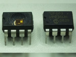
 Copy Microcontroller PIC16F684 Firmware
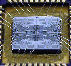
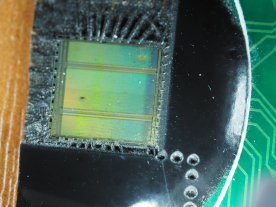
Copy Microcontroller PIC16F684 Firmware needs to unlock Microprocessor PIC16F684 security fuse bit, the silicon package can be removed by proper chemical solution, by focus ion beam will effectively modify the circuitry pattern of MCU PIC16F684
Copy Microcontroller PIC16F684 Firmware needs to unlock Microprocessor PIC16F684 security fuse bit, the silicon package can be removed by proper chemical solution, by focus ion beam will effectively modify the circuitry pattern of MCU PIC16F684;
High-Performance RISC CPU:
· Only 35 instructions to learn:
– All single-cycle instructions except branches
· Operating speed:
– DC – 20 MHz oscillator/clock input
– DC – 200 ns instruction cycle
· Interrupt capability
· 8-level deep hardware stack
Low-Power Features:
· Standby Current:
– 1 nA @ 2.0V, typical
· Operating Current:
– 8.5 µA @ 32 kHz, 2.0V, typical
– 100 µA @ 1 MHz, 2.0V, typical
· Watchdog Timer Current:
– 1 µA @ 2.0V, typical
· Direct, Indirect and Relative Addressing modes
Peripheral Features:
Special Microcontroller Features:
· Precision Internal Oscillator:
– Factory calibrated to ±1%
– Software selectable frequency range of 8 MHz to 31 kHz
– Software tunable
– Two-speed Start-up mode
– Crystal fail detect for critical applications
– Clock mode switching during operation for power savings
· Power-saving Sleep mode
· Wide operating voltage range (2.0V-5.5V)
· Industrial and Extended Temperature range
· Power-on Reset (POR)
· Power-up Timer (PWRT) and Oscillator Start-up Timer (OST)
· Brown-out Detect (BOD) with software control option
· Enhanced low-current Watchdog Timer (WDT) with on-chip oscillator (software selectable nominal 268 seconds with full prescaler) with software enable;
· Multiplexed Master Clear with pull-up/input pin
· Programmable code protection
· High Endurance Flash/EEPROM cell:
– 100,000 write Flash endurance
– 1,000,000 write EEPROM endurance
– Flash/Data EEPROM retention: > 40 years
· 12 I/O pins with individual direction control:
– High current source/sink for direct LED drive
– Interrupt-on-pin change
– Individually programmable weak pull-ups
– Ultra Low-power Wake-up (ULPWU)
· Analog comparator module with:
– Two analog comparators
– Programmable on-chip voltage reference (CVREF) module (% of VDD)
– Comparator inputs and outputs externally accessible
· A/D Converter:
– 10-bit resolution and 8 channels
· Timer0: 8-bit timer/counter with 8-bit programmable prescaler· Enhanced Timer1:
– 16-bit timer/counter with prescaler
– External Gate Input mode
– Option to use OSC1 and OSC2 in LP mode as Timer1 oscillator if INTOSC mode selected
· Timer2: 8-bit timer/counter with 8-bit period register, prescaler and postscaler
· Enhanced Capture, Compare, PWM module:
– 16-bit Capture, max resolution 12.5 ns
– Compare, max resolution 200 ns
– 10-bit PWM with 1, 2 or 4 output channels, programmable “dead time”, max frequency 20 kHz
· In-Circuit Serial ProgrammingTM (ICSPTM) via two pins.
Copy MCU PIC32MX440F512H Binary
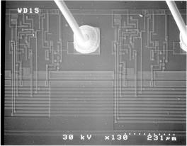
Copy MCU PIC32MX440F512H Binary and rewrite the firmware from master Microcontroller PIC32MX440F512H to blank new Microprocessor, decapsulate the MCU PIC32MX440F512H and get access to the databus is the first step of MCU cracking;
High-Performance 32-bit RISC CPU:
· MIPS32® M4K® 32-bit core with 5-stage pipeline
· 80 MHz maximum frequency
· 1.56 DMIPS/MHz (Dhrystone 2.1) performance at 0 wait state Flash access
· Single-cycle multiply and high-performance divide unit
· MIPS16e® mode for up to 40% smaller code size
· Two sets of 32 core register files (32-bit) to reduce interrupt latency
· Prefetch Cache module to speed execution
· Operating temperature range of -40ºC to +105ºC
· Operating voltage range of 2.3V to 3.6V
· 32K to 512K Flash memory (plus an additional 12 KB of boot Flash)
· 8K to 32K SRAM memory
· Pin-compatible with most PIC24/dsPIC® DSC devices
· Multiple power management modes
· Multiple interrupt vectors with individually programmable priority
· Fail-Safe Clock Monitor Mode
· Configurable Watchdog Timer with on-chip Low-Power RC Oscillator for reliable operation
Peripheral Features:
· Atomic SET, CLEAR and INVERT operation on select peripheral registers
· Up to 4-channel hardware DMA with automatic data size detection
· USB 2.0-compliant full-speed device and On-The-Go (OTG) controller
· USB has a dedicated DMA channel
· 3 MHz to 25 MHz crystal oscillator
· Internal 8 MHz and 32 kHz oscillators
· Separate PLLs for CPU and USB clocks
· Two I2C™ modules
· Two UART modules with:
– RS-232, RS-485 and LIN support
– IrDA® with on-chip hardware encoder and decoder
· Up to two SPI modules
· Parallel Master and Slave Port (PMP/PSP) with 8-bit and 16-bit data and up to 16 address lines
· Hardware Real-Time Clock and Calendar (RTCC)
· Five 16-bit Timers/Counters (two 16-bit pairs combine to create two 32-bit timers)
· Five capture inputs
· Five compare/PWM outputs
· Five external interrupt pins
· High-Speed I/O pins capable of toggling at up to 80 MHz
· High-current sink/source (18 mA/18 mA) on all I/O pins
· Configurable open-drain output on digital I/O pins
Debug Features:
· Two programming and debugging Interfaces:
– 2-wire interface with unintrusive access and real-time data exchange with application
– 4-wire MIPS® standard enhanced JTAG interface
· Unintrusive hardware-based instruction trace
· IEEE Standard 1149.2-compatible (JTAG) boundary scan
Analog Features:
· Up to 16-channel 10-bit Analog-to-Digital Converter:
– 1000 ksps conversion rate
– Conversion available during Sleep, Idle
· Two Analog Comparators
Recover IC STM32F107RCT6 Code
Recover IC STM32F107RCT6 code from MCU STM32F107RCT6 program memory, use MCU cracking technique to remove the security fuse by focus ion beam
Recover IC STM32F107RCT6 code from MCU STM32F107RCT6 program memory, use MCU cracking technique to remove the security fuse by focus ion beam;
Core: ARM 32-bit Cortex™-M3 CPU
– 72 MHz maximum frequency, 1.25 DMIPS/MHz (Dhrystone 2.1) performance at 0 wait state memory
LQFP100 14 × 14 mm
LQFP64 10 × 10 mm
LFBGA100 10 × 10 mm
– Single-cycle multiplication and hardware division
Memories
– 64 to 256 Kbytes of Flash memory
– 64 Kbytes of general-purpose SRAM Clock, reset and supply management
– 2.0 to 3.6 V application supply and I/Os
– POR, PDR, and programmable voltage detector (PVD)
– 3-to-25 MHz crystal oscillator
– Internal 8 MHz factory-trimmed RC
– Internal 40 kHz RC with calibration
– 32 kHz oscillator for RTC with calibration
Low power
– Sleep, Stop and Standby modes
– VBAT supply for RTC and backup registers 2 × 12-bit, 1 µs A/D converters (16 channels)
– Conversion range: 0 to 3.6 V
– Sample and hold capability
– Temperature sensor
– up to 2 MSPS in interleaved mode 2 × 12-bit D/A converters DMA: 12-channel DMA controller
– Supported peripherals: timers, ADCs, DAC, I2Ss, SPIs, I2Cs and USARTs
Up to 10 timers with pinout remap capability
– Up to four 16-bit timers, each with up to 4 IC/OC/PWM or pulse counter and quadrature (incremental) encoder input
– 1 × 16-bit motor control PWM timer with dead-time generation and emergency stop
– 2 × watchdog timers (Independent and Window)
– SysTick timer: a 24-bit downcounter
– 2 × 16-bit basic timers to drive the DAC Up to 14 communication interfaces with pinout remap capability
– Up to 2 × I2C interfaces (SMBus/PMBus)
– Up to 5 USARTs (ISO 7816 interface, LIN, IrDA capability, modem control)
– Up to 3 SPIs (18 Mbit/s), 2 with a multiplexed I2S interface that offers audio class accuracy via advanced PLL schemes
– 2 × CAN interfaces (2.0B Active) with 512 bytes of dedicated SRAM
– USB 2.0 full-speed device/host/OTG controller with on-chip PHY that supports
HNP/SRP/ID with 1.25 Kbytes of dedicated SRAM
– 10/100 Ethernet MAC with dedicated DMA and SRAM (4 Kbytes): IEEE1588 hardware support, MII/RMII available on all packages
– Cortex-M3 Embedded Trace Macrocell™ Up to 80 fast I/O ports
– 51/80 I/Os, all mappable on 16 external interrupt vectors and almost all 5 V-tolerant CRC calculation unit, 96-bit unique ID
Copy IC ATmega8L Heximal
Copy IC Atmega8L Heximal from MCU ATmega8L flash memory, crack MCU protective system and disable its security fuse bit, the status of Microcontroller ATmega8L will be modified from locked to unlocked one
Copy IC Atmega8L Heximal from MCU ATmega8L flash memory, crack MCU ATmega8L protective system and disable its security fuse bit, the status of Microcontroller ATmega8L will be modified from locked to unlocked one;
High-performance, Low-power AVR 8-bit Microcontroller
· Advanced RISC Architecture
– 130 Powerful Instructions – Most Single-clock Cycle Execution
– 32 x 8 General Purpose Working Registers
– Fully Static Operation
– Up to 16 MIPS Throughput at 16 MHz
– On-chip 2-cycle Multiplier
High Endurance Non-volatile Memory segments
– 8K Bytes of In-System Self-programmable Flash program memory
– 512 Bytes EEPROM
– 1K Byte Internal SRAM
– Write/Erase Cycles: 10,000 Flash/100,000 EEPROM (1)(3)
– Data retention: 20 years at 85°C/100 years at 25°C (2)(3)
– Optional Boot Code Section with Independent Lock Bits
In-System Programming by On-chip Boot Program True Read-While-Write Operation
– Programming Lock for Software Security
Peripheral Features
– Two 8-bit Timer/Counters with Separate Prescaler, one Compare Mode
– One 16-bit Timer/Counter with Separate Prescaler, Compare Mode, and Capture Mode
– Real Time Counter with Separate Oscillator
– Three PWM Channels
– 8-channel ADC in TQFP and QFN/MLF package
Eight Channels 10-bit Accuracy
– 6-channel ADC in PDIP package
Six Channels 10-bit Accuracy
– Byte-oriented Two-wire Serial Interface
– Programmable Serial USART
– Master/Slave SPI Serial Interface
– Programmable Watchdog Timer with Separate On-chip Oscillator
– On-chip Analog Comparator
Special Microcontroller Features
– Power-on Reset and Programmable Brown-out Detection
– Internal Calibrated RC Oscillator
– External and Internal Interrupt Sources
– Five Sleep Modes: Idle, ADC Noise Reduction, Power-save, Power-down, and Standby I/O and Packages
– 23 Programmable I/O Lines
– 28-lead PDIP, 32-lead TQFP, and 32-pad QFN/MLF Operating Voltages
– 2.7 – 5.5V (ATmega8L)
– 4.5 – 5.5V (ATmega8) Speed Grades
– 0 – 8 MHz (ATmega8L)
– 0 – 16 MHz (ATmega8)
Power Consumption at 4 Mhz, 3V, 25°C
– Active: 3.6 mA
– Idle Mode: 1.0 mA
– Power-down Mode: 0.5 µA
Attack Chip dsPIC33FJ256GP506A Software
Attack Chip dsPIC33FJ256GP506A and compromise Microcontroller dsPIC33FJ256GP506 tamper resistance system, readout MCU software from dsPIC33FJ256 flash and eeprom memory
Attack Chip dsPIC33FJ256GP506A and compromise Microcontroller dsPIC33FJ256GP506 tamper resistance system, readout MCU software from dsPIC33FJ256 flash and eeprom memory;
Operating Conditions
· 3.0V to 3.6V, -40ºC to +150ºC, DC to 20 MIPS
· 3.0V to 3.6V, -40ºC to +125ºC, DC to 40 MIPS
Core: 16-bit dsPIC33F CPU
Timers/Output Compare/Input Capture
· Up to nine 16-bit timers/counters. Can pair up to make four 32-bit timers;
· Eight Output Compare modules configurable as timers/counters;
Code-efficient (C and Assembly) architecture
Two 40-bit wide accumulators
Single-cycle (MAC/MPY) with dual data fetch
Single-cycle mixed-sign MUL plus hardware divide
· Eight Input Capture modules
Communication Interfaces
· Two UART modules (10 Mbps)
– With support for LIN 2.0 protocols and IrDA®
· Two 4-wire SPI modules (15 Mbps)
Clock Management
· Up to two I2C™ modules (up to 1 Mbaud) with ±2% internal oscillator
Programmable PLLs and oscillator clock sources
Fail-Safe Clock Monitor (FSCM)
Independent Watchdog Timer (WDT)
Fast wake-up and start-up
SMBus support
· Up to two Enhanced CAN (ECAN) modules (1 Mbaud) with 2.0B support
· Data Converter Interface (DCI) module with I2S codec support
Power Management
· Low-power management modes (Sleep, Idle, Doze)
· Integrated Power-on Reset and Brown-out Reset
· 2.1 mA/MHz dynamic current (typical)
· 50 μA IPD current (typical)
Advanced Analog Features
· Two ADC modules:
– Configurable as 10-bit, 1.1 Msps with four S&H or 12-bit, 500 ksps with one S&H
– 18 analog inputs on 64-pin devices and up to 32 analog inputs on 100-pin devices
· Flexible and independent ADC trigger sources
Input/Output
· Sink/Source up to 10 mA (pin specific) for standard VOH/VOL, up to 16 mA (pin specific) for non-standard VOH1
· 5V-tolerant pins
· Selectable open drain, pull-ups, and pull-downs
· Up to 5 mA overvoltage clamp current
· External interrupts on all I/O pins
Qualification and Class B Support
· AEC-Q100 REVG (Grade 1 -40ºC to +125ºC)
· AEC-Q100 REVG (Grade 0 -40ºC to +150ºC)
· Class B Safety Library, IEC 60730
Debugger Development Support
Packages
In-circuit and in-application programming
Two program and two complex data breakpoints
IEEE 1149.2-compatible (JTAG) boundary scan
Trace and run-time watch
Attack Microcontroller ST62T15C6 firmware
Attack Microcontroller ST62T15C6 protective system and extract firmware from MCU ST62T15 memory, the whole tamper resistance system will be disable by Microprocessor unlocking technique
Attack Microcontroller ST62T15C6 protective system and extract firmware from MCU ST62T15 memory, the whole tamper resistance system will be disable by Microprocessor unlocking technique;
Memories
– 2K or 4K bytes Program memory (OTP, EPROM, FASTROM or ROM) with read-out protection
– 64 bytes RAM
Clock, Reset and Supply Management
– Enhanced reset system
– Low Voltage Detector (LVD) for Safe Reset
– Clock sources: crystal/ceramic resonator or RC network, external clock, backup oscillator (LFAO)
– Oscillator Safeguard (OSG)
– 2 Power Saving Modes: Wait and Stop
Interrupt Management
– 4 interrupt vectors plus NMI and RESET
– 20 external interrupt lines (on 2 vectors)
– 1 external non-interrupt line
– 20 multifunctional bidirectional I/O lines
– 16 alternate function lines
– 4 high sink outputs (20mA)
– Configurable watchdog timer
– 8-bit timer/counter with a 7-bit prescaler
Analog Peripheral
– 8-bit ADC with 16 input channels
Instruction Set
– 8-bit data manipulation
– 40 basic instructions
– 9 addressing modes
– Bit manipulation
The ST6215C, 25C devices are low cost members mable option bytes of the OTP/EPROM versions of the ST62xx 8-bit family of microcontrol-in the ROM option list applications. All ST62xx devices are based on a building block approach: a common core is surrounded by a number of on-chip peripherals for the purpose of IC program hacking.
Circuit Engineering Company Limited continues to be recognized as the Southern China Leader in Services for IC Break, MCU attack, Chip Recover, Microcontroller Copy service. With the advancement of today’s modern circuit board technology, it is more important than ever to have specialists available to help you at a moment’s notice. Our engineering and commercial teams collectively have a vast amount of electronic experience covering field include Consumer Electronics, Industrial Automation Electronics, Wireless Communication Electronics., etc. For more information please contact us through email.
Attack MCU MSP430G2452IPW14R Heximal
Attack MCU MSP430G2452IPW14R flash memory and extract heximal from Microcontroller MSP430G2452, the status of Microprocessor will be reset from locked to open one after get access to the databus
Attack MCU MSP430G2452IPW14R flash memory and extract heximal from Microcontroller MSP430G2452, the status of Microprocessor will be reset from locked to open one after get access to the databus;
FEATURES
Low Supply Voltage Range: 1.8 V to 3.6 V
Ultra-Low Power Consumption
– Active Mode: 220 µA at 1 MHz, 2.2 V
– Standby Mode: 0.5 µA
– Off Mode (RAM Retention): 0.1 µA
Five Power-Saving Modes
Ultra-Fast Wake-Up From Standby Mode in Less Than 1 µs
16-Bit RISC Architecture, 62.5-ns Instruction Cycle Time Basic Clock Module Configurations
– Internal Frequencies up to 16 MHz With
Four Calibrated Frequencies
– Internal Very-Low-Power Low-Frequency (LF) Oscillator
– 32-kHz Crystal
– External Digital Clock Source
One 16-Bit Timer_A With Three Capture/Compare Registers
Up to 16 Touch-Sense Enabled I/O Pins
Universal Serial Interface (USI) Supporting SPI and I2C
10-Bit 200-ksps Analog-to-Digital (A/D)
Converter With Internal Reference, Sample-and-Hold, and Autoscan (MSP430G2x52 Only)
On-Chip Comparator for Analog
Brownout Detector Serial Onboard Programming,
No External Programming Voltage Needed,
Programmable Code Protection by Security Fuse
On-Chip Emulation Logic With Spy-Bi-Wire Interface
Family Members are Summarized in Table 1 Package Options
– TSSOP: 14 Pin, 20 Pin
– PDIP: 20 Pin
– QFN: 16 Pin
For Complete Module Descriptions, See the MSP430x2xx Family User’s Guide (SLAU144)
Attack IC TMS320F28232PGFA Software
Attack IC TMS320F28232PGFA DSP MCU, reset the status of DSP Microcontroller TMS320F28232PGFA from locked to unlocked one through MCU cracking process, software of MCU’s flash memory can readout;
Attack IC TMS320F28232PGFA DSP MCU, reset the status of DSP Microcontroller TMS320F28232PGFA from locked to unlocked one through MCU cracking process, software of MCU’s flash memory can readout
· High-Performance Static CMOS Technology
– Up to 150 MHz (6.67-ns Cycle Time)
– 1.9-V/1.8-V Core, 3.3-V I/O Design
· High-Performance 32-Bit CPU (TMS320C28x)
– IEEE-754 Single-Precision Floating-Point
Unit (FPU) (F2833x only)
– 16 x 16 and 32 x 32 MAC Operations
– 16 x 16 Dual MAC
– Harvard Bus Architecture
– Fast Interrupt Response and Processing
– Unified Memory Programming Model
– Code-Efficient (in C/C++ and Assembly)
· Six-Channel DMA Controller (for ADC, McBSP, ePWM, XINTF, and SARAM)
· 16-Bit or 32-Bit External Interface (XINTF)
– Over 2M x 16 Address Reach
· On-Chip Memory
– F28335, F28235: 256K x 16 Flash, 34K x 16 SARAM
– F28334, F28234: 128K x 16 Flash, 34K x 16 SARAM
– F28332, F28232: 64K x 16 Flash, 26K x 16 SARAM
– 1K x 16 OTP ROM
· Boot ROM (8K x 16)
– With Software Boot Modes (via SCI, SPI, CAN, I2C, McBSP, XINTF, and Parallel I/O)
– Standard Math Tables
· Clock and System Control
– Dynamic PLL Ratio Changes Supported
– On-Chip Oscillator
– Watchdog Timer Module
· GPIO0 to GPIO63 Pins Can Be Connected to One of the Eight External Core Interrupts
· Peripheral Interrupt Expansion (PIE) Block That Supports All 58 Peripheral Interrupts
· 128-Bit Security Key/Lock
– Protects Flash/OTP/RAM Blocks
– Prevents Firmware Reverse Engineering
· Enhanced Control Peripherals
– Up to 18 PWM Outputs
– Up to 6 HRPWM Outputs With 150 ps MEP Resolution
– Up to 6 Event Capture Inputs
– Up to 2 Quadrature Encoder Interfaces
– Up to 8 32-Bit Timers
(6 for eCAPs and 2 for eQEPs)
– Up to 9 16-Bit Timers
(6 for ePWMs and 3 XINTCTRs)
· Three 32-Bit CPU Timers
· Serial Port Peripherals
– Up to 2 CAN Modules
– Up to 3 SCI (UART) Modules
– Up to 2 McBSP Modules (Configurable as SPI)
– One SPI Module
– One Inter-Integrated-Circuit (I2C) Bus
· 12-Bit ADC, 16 Channels
– 80-ns Conversion Rate
– 2 x 8 Channel Input Multiplexer
– Two Sample-and-Hold
– Single/Simultaneous Conversions
– Internal or External Reference
· Up to 88 Individually Programmable, Multiplexed GPIO Pins With Input Filtering
· JTAG Boundary Scan Support (1)
· Advanced Emulation Features
– Analysis and Breakpoint Functions
– Real-Time Debug via Hardware
· Development Support Includes
– ANSI C/C++ Compiler/Assembler/Linker
– Code Composer Studio™ IDE
– DSP/BIOS™
– Digital Motor Control and Digital Power Software Libraries
Low-Power Modes and Power Savings
– IDLE, STANDBY, HALT Modes Supported
– Disable Individual Peripheral Clocks
· Endianness: Little Endian
· Package Options:
– Lead-free, Green Packaging
– Low-Profile Quad Flatpack (PGF, PTP)
– MicroStar BGA™ (ZHH)
– Plastic BGA (ZJZ)
· Temperature Options:
– A: –40°C to 85°C (PGF, ZHH, ZJZ)
– S: –40°C to 125°C (PTP, ZJZ)
– Q: –40°C to 125°C (PTP, ZJZ)
Recover IC ST62T65C6 Software
Recover IC ST62T65C6 Software from MCU ST62T65C6 flash memory, reset the security fuse bit status by focus ion beam technique which is the most important part for microcontroller unlocking, readout firmware from MCU
Recover IC ST62T65C6 Software from MCU ST62T65C6 flash memory, reset the security fuse bit status by focus ion beam technique which is the most important part for microcontroller unlocking, readout firmware from MCU;
Features
■ 3.0 to 6.0V supply operating range
■ 8 MHz maximum clock frequency
■ -40 to +125°C operating temperature range
■ Run, Wait and Stop modes
■ 5 interrupt vectors
■ Look-up table capability in program memory
■ Data storage in program memory: user selectable size
■ Data RAM: 128 bytes
■ Data EEPROM: 128 bytes (not in ST6255C)
■ User programmable options
■ 21 I/O pins, fully programmable as:
– Input with pull-up resistor
– Input without pull-up resistor
– Input with interrupt generation
– Open-drain or push-pull output
– Analog Input
■ 8 I/O lines can sink up to 30 mA to drive LEDs or TRIACs directly
– 8-bit Timer/Counter with 7-bit programmable prescaler
■ 8-bit Auto-reload timer with 7-bit programmable prescaler (AR Timer)
■ Digital watchdog
■ Oscillator safe guard (not in ST6265B ROM devices)
■ Low voltage detector for safe reset (not in ST6265B ROM devices)
■ 8-bit A/D converter with 13 analog inputs
■ 8-bit synchronous peripheral interface (SPI)
■ On-chip clock oscillator can be driven by quartz crystal, ceramic resonator or RC network
■ User configurable power-on reset
(See end of Datasheet for Ordering Information)
Table 1. Device summary
■ One external non-maskable interrupt
■ ST626x-EMU2 Emulation and Development
System (connects to an MS-DOS PC via a parallel port)
Circuit Engineering Company Limited continues to be recognized as the Southern China Leader in Services for read IC, MCU recovery, Chip decrypt, Microcontroller copy service. With the advancement of today’s modern circuit board technology, it is more important than ever to have specialists available to help you at a moment’s notice. Our engineering and commercial teams collectively have a vast amount of electronic experience covering field include Consumer Electronics, Industrial Automation Electronics, Wireless Communication Electronics., etc. For more information please contact us through email.
Read Microcontroller HT68F40 Heximal
Read Microcontroller HT68F40 Heximal from flash memory, and then copy MCU HT68F40 code to new MCU which will provide the same functions as master microcomputer HT68F40 by crack Microprocessor security fuse bit;
Read Microcontroller HT68F40 Heximal from flash memory, and then copy MCU HT68F40 code to new MCU which will provide the same functions as master microcomputer HT68F40 by crack Microprocessor security fuse bit;
Features
CPU Features
· Operating Voltage:
Peripheral Features
· Flash Program Memory: 1K´14 ~ 12K´16
fSYS= 8MHz: 2.2V~5.5V
fSYS= 12MHz: 2.7V~5.5V
fSYS= 20MHz: 4.5V~5.5V
Up to 0.2ms instruction cycle with 20MHz system clock at VDD=5V
Power down and wake-up functions to reduce power consumption
Five oscillators:
External Crystal – HXT
External 32.768kHz Crystal – LXT
· RAM Data Memory: 64´8 ~ 576´8
· EEPROM Memory: 32´8~256´8
· Watchdog Timer function
· Up to 50 bidirectional I/O lines
· Software controlled 4-SCOM lines LCD driver with 1/2 bias
· Multiple pin-shared external interrupts
· Multiple Timer Module for time measure, input capture, compare match output, PWM output
External RC – ERC
Internal RC – HIRC
Internal 32kHz RC – LIRC
single pulse output function
Serial Interfaces Module – SIM for SPI or I2C
Dual Comparator functions
Multi-mode operation: NORMAL, SLOW, IDLE and SLEEP
Fully integrated internal 4MHz, 8MHz and 12MHz
Dual Time-Base functions for generation of fixed time interrupt signals
Low voltage reset function oscillator requires no external components
All instructions executed in one or two instruction cycles
Table read instructions
63 powerful instructions
Up to 12-level subroutine nesting
Bit manipulation instruction
· Low voltage detect function
· Wide range of available package types
General Description
The HT68FXX series of devices are Flash Memory I/O type 8-bit high performance RISC architecture microcontrollers. Offering users the convenience of Flash Memory multi-programming features, these devices also include a wide range of functions and features. Other memory includes an area of RAM Data Memory as well as an area of EEPROM memory for storage of non-volatile data such as serial numbers, calibration data etc for the purpose of read Microcontroller.
Multiple and extremely flexible Timer Modules provide timing, pulse generation and PWM generation functions. Analog features include dual comparator functions. Communication with the outside world is catered for by including fully integrated SPI or I2C interface functions, two popular interfaces which provide designers with a means of easy communication with external peripheral hardware. Protective features such as an internal Watchdog Timer, Low Voltage Reset and Low Voltage Detector coupled with excellent noise immunity and ESD protection ensure that reliable operation is maintained in hostile electrical environments.
A full choice of HXT, LXT, ERC, HIRC and LIRC oscillator functions are provided including a fully integrated system oscillator which requires no external components for its implementation. The ability to operate and switch dynamically between a range of operating modes using different clock sources gives users the ability to optimise microcontroller operation and minimise power consumption.
The inclusion of flexible I/O programming features, Time-Base functions along with many other features ensure that the devices will find excellent use in applications such as electronic metering, environmental monitoring, handheld instruments, household appliances, electronically controlled tools, motor driving in addition to many others.