 Reverse IC ATmega861V Code
Reverse IC ATmega861V code programming process, disable the protective measurement by unlock microcontroller ATmega861V, extract content from MCU program memory and reprogramme the firmware to new ATmega861V;
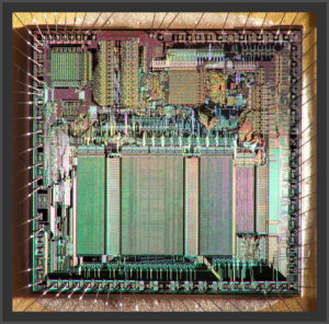
Reverse IC ATmega861V code programming process, disable the protective measurement by unlock microcontroller ATmega861V, extract content from MCU program memory and reprogramme the firmware to new ATmega861V
The Compare Output mode (COM2x1:0) bits have two functions. The Waveform Generator uses the COM2x1:0 bits for defining the Output Compare (OC2x) state at the next compare match.
Also, the COM2x1:0 bits control the OC2x pin output source. Figure 70 shows a simplified schematic of the logic affected by the COM2x1:0 bit setting. The I/O Registers, I/O bits, and I/O pins in the figure are shown in bold. Only the parts of the general I/O Port Control Registers (DDR and PORT) that are affected by the COM2x1:0 bits are shown if breaking Microcontroller PIC16C65B eeprom.
When referring to the OC2x state, the reference is for the internal OC2x Register, not the OC2x pin. The general I/O port function is overridden by the Output Compare (OC2x) from the Waveform Generator if either of the COM2x1:0 bits are set.
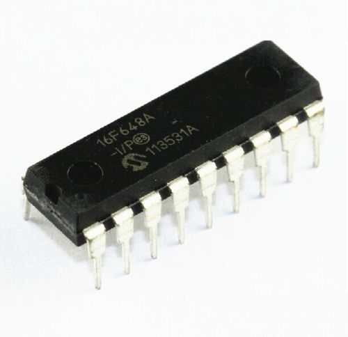
decode microprocessor PIC16F648A flash memory and extract heximal data from its memory
However, the OC2x pin direction (input or output) is still controlled by the Data Direction Register (DDR) for the port pin. The Data Direction Register bit for the OC2x pin (DDR_OC2x) must be set as output before the OC2x value is visible on the pin. The port override function is independent of the Waveform Generation mode.
The design of the Output Compare pin logic allows initialization of the OC2x state before the output is enabled. Note that some COM2x1:0 bit settings are reserved for certain modes of operation. See “8-bit Timer/Counter Register Description” on page 184 if Recover MCU PIC16F687 software code.
The Waveform Generator uses the COM2x1:0 bits differently in normal, CTC, and PWM modes. For all modes, setting the COM2x1:0 = 0 tells the Waveform Generator that no action on the OC2x Register is to be performed on the next compare match.
For compare output actions in the non-PWM modes refer to Table 88 on page 185. For fast PWM mode, refer to Table 89 on page 185, and for phase correct PWM refer to Table 90 on page 186. A change of the COM2x1:0 bits state will have effect at the first compare match after the bits are written. For non-PWM modes, the action can be forced to have immediate effect by using the FOC2x strobe bits.