 Recover MCU ATmega1280P Eeprom
Recover MCU ATmega1280P Eeprom content as well as flash program in the format of binary or heximal and copy the firmware to new microcontroller atmega1280p;
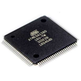
Recover MCU ATmega1280P Eeprom content as well as flash program in the format of binary or heximal and copy the firmware to new microcontroller atmega1280p;
The N variable represents the prescale factor (1, 8, 64, 256, or 1024). The extreme values for the OCR0A Register represent special cases when generating a PWM waveform output in the phase correct PWM mode. If the OCR0A is set equal to BOTTOM, the output will be continuously low and if set equal to MAX the output will be continuously high for non-inverted PWM mode. For inverted PWM the output will have the opposite logic values.
crack atmega1280p microprocessor fuse bit and readout embedded firmware from flash memory and eeprom memory
At the very start of period 2 in Figure 44 OCnx has a transition from high to low even though there is no Compare Match. The point of this transition is to guarantee symmetry around BOTTOM. There are two cases that give a transition without Compare Match. OCR0A changes its value from MAX, like in Figure 44. When the OCR0A value is MAX the OCn pin value is the same as the result of a down-counting Compare Match.
To ensure symmetry around BOTTOM the OCn value at MAX must correspond to the result of an up-counting Compare Match. The timer starts counting from a value higher than the one in OCR0A, and for that reason misses the Compare Match and hence the OCn change that would have happened on the way up. The Timer/Counter is a synchronous design and the timer clock (clkT0) is therefore shown as a clock enable signal in the following figures. The figures include information on when Interrupt Flags are set. Figure 45 contains timing data for basic Timer/Counter operation.
The figure shows the count sequence close to the MAX value in all modes other than phase correct PWM mode. These bits control the Output Compare pin (OC0B) behavior to recover atmega1280 mcu embedded heximal file. If one or both of the COM0B1:0 bits are set, the OC0B output overrides the normal port functionality of the I/O pin it is connected.
However, note that the Data Direction Register (DDR) bit corresponding to the OC0B pin must be set in order to enable the output driver. When OC0B is connected to the pin, the function of the COM0B1:0 bits depends on the WGM02:0 bit setting. Table 70 shows the COM0A1:0 bit functionality when the WGM02:0 bits are set to a normal or CTC mode (non-PWM).
Combined with the WGM02 bit found in the TCCR0B Register, these bits control the counting sequence of the counter, the source for maximum (TOP) counter value, and what type of waveform generation to be used. Modes of operation supported by the Timer/Counter unit are: Normal mode (counter), Clear Timer on Compare Match (CTC) mode, and two types of Pulse Width Modulation (PWM) modes.