 Decrypt Locked Chip PIC12F508 Firmware
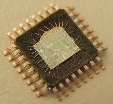
Decrypt Locked Chip PIC12F508 Firmware from secured program memory and data memory, microcontroller PIC12F508 cracking will help to disable the protection and readout MCU PIC12F508 heximal.
The code for these functions is available on our website www.microchip.com. The code will be accessed by either including the source code FL51XINC.ASM or by linking FLASH5IX.ASM.
It is very important to check the return codes when using these calls, and retry the operation if unsuccessful. Unsuccessful return codes occur when the EE data memory is busy with the previous write, which can take up to 4 mS if copy chip pic16c73a program.
SDA is a bi-directional pin used to transfer addresses and data into and data out of the device. For normal data transfer SDA is allowed to change only during SCL low. Changes during SCL high are reserved for indicating the START and STOP conditions.
The EEPROM interface is a 2-wire bus protocol consisting of data (SDA) and a clock (SCL). Although these lines are mapped into the GPIO register, they are not accessible as external pins; only to the internal EEPROM peripheral after recover mcu pic16f74a binary.
SDA and SCL operation is also slightly different than GPO-GP5 as listed below. Namely, to avoid code overhead in modifying the TRIS register, both SDA and SCL are always outputs.
To decrypt data from the EEPROM peripheral requires outputting a ‘1’ on SDA placing it in high-Z state, where only the internal 100K pull-up is active on the SDA line.
This code must reside in the lower half of a page. The code achieves it’s small size without additional calls through the use of a sequencing table. The table is a list of procedures that must be called in order.
The table uses an ADDWF PCL,F instruction, effectively a computed goto, to sequence to the next procedure. However the ADDWF PCL,F instruction yields an 8 bit address after recover chip pic16c71 code,
The following bus protocol is to be used with the EEPROM data memory.
Data transfer may be initiated only when the bus is not busy.
During data transfer, the data line must remain stable whenever the clock line is HIGH. Changes in the data line while the clock line is HIGH will be interpreted as a period of the clock signal. There is one bit of data per clock pulse.
Each data transfer is initiated with a START condition and terminated with a STOP condition. The number of the data bytes transferred between the START and STOP conditions is determined by the master device and is theoretically unlimited if Decrypt locked Chip Firmware. A HIGH to LOW transition of the SDA line while the clock (SCL) is HIGH determines a START condition. All commands must be preceded by a START condition. A LOW to HIGH transition of the SDA line while the clock (SCL) is HIGH determines a STOP condition. All operations must be ended with a STOP condition.