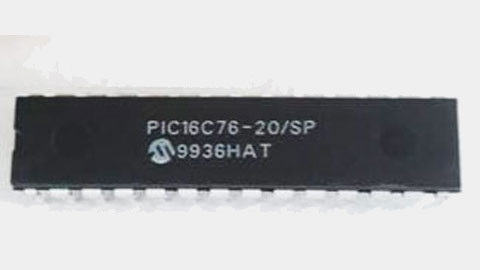
 Copy Microcontroller PIC16C76 Heximal
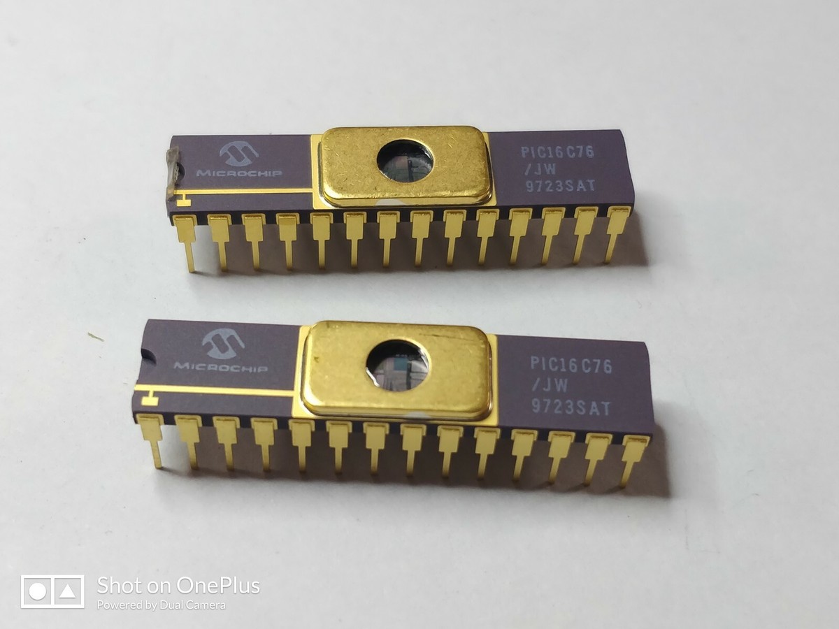
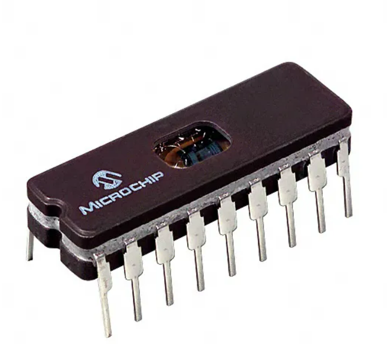
The Microchip PIC16C76 is a classic 8-bit microcontroller that continues to operate in a wide range of industrial and commercial products. When customers search for Copy Microcontroller PIC16C76 Heximal, it is usually because the original source code, program, or compiled firmware has been lost, yet the hardware remains essential to daily operations. Our professional recovery service is designed to help authorized owners retrieve, clone, or duplicate the internal heximal and binary content from protected and secured PIC16C76 devices—without exposing sensitive technical details.
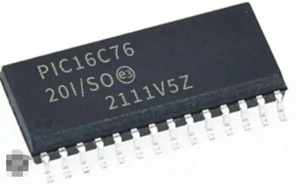
We can Copy Microcontroller PIC16C76 Heximal, please view the Microcontroller PIC16C76 features for your reference:
Any instruction which writes, operates internally as a read followed by a write operation. The BCF and BSF instructions, for example, read the register into the CPU, execute the bit operation and write the result back to the register.
Thanks to its stable architecture, integrated peripherals, and reliable embedded design, the PIC16C76 has been widely used in:
- Industrial automation controllers and monitoring systems
- Measurement instruments and data acquisition devices
- Motor control and power management modules
- Consumer electronics and appliance controllers
- Educational platforms and OEM-specific embedded products
In these applications, critical operational logic and calibration data are stored in internal flash, EEPROM, and memory areas. Once these regions become locked or encrypted, standard programmers are unable to access the internal archive, creating major risks for maintenance and production continuity.
Caution must be used when these instructions are applied to a port with both inputs and outputs defined. For example, a BSF operation on bit5 of PORTB will cause all eight bits of PORTB to be read into the CPU.
Our service supports legitimate clients who need to attack access barriers in order to recover their own intellectual property. We help customers break through protective security mechanisms and safely decode the embedded program stored within the microcontroller.
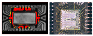
Depending on the device condition and security configuration, recovery may involve controlled analysis, advanced inspection, or authorized decapsulation. The final result is a verified file containing the recovered firmware, delivered as a binary or heximal image suitable for archiving, system migration, or controlled duplication. We do not disclose how the recovery is performed, and we do not provide instructions on how to hack devices.

Then the BSF operation takes place on bit5 and PORTB is written to the output latches. If another bit of PORTB is used as a bi-directional I/O pin (e.g., bit0) and it is defined as an input at this time, the input signal present on the pin itself would be read into the CPU and rewritten to the data latch of this particular pin, overwriting the previous content.
Organizations rely on this service for several important reasons:
- Restoring production when original source code is unavailable
- Avoiding costly redesign of proven legacy hardware
- Creating a secure archive for long-term product support
- Enabling accurate system clone or duplicate manufacturing
- Protecting existing engineering investment and operational know-how
Recovered firmware allows businesses to extend product life cycles, reduce downtime, and maintain control over their embedded systems.
As long as the pin stays in the input mode, no problem occurs. However, if bit0 is switched to an output, the content of the data latch may now be unknown.
Reading the port register, reads the values of the port pins. Writing to the port register writes the value to the port latch. When using read-modify-write instructions (ex.BCF, BSF, etc.) on a port, the value of the port pins is read, the desired operation is done to this value, and this value is then written to the port latch.
Example 5-4 shows the effect of two sequential read-modify-write instructions on an I/O port. A pin actively outputting a Low or High should not be driven from external devices at the same time in order to change the level on this pin (“wired-or”, “wired-and”). The resulting high output currents may damage the chip.
The actual write to an I/O port happens at the end of an instruction cycle, whereas for reading, the data must be valid at the beginning of the instruction cycle (Figure 5-10). Therefore, care must be exercised if a write followed by a read operation is carried out on the same I/ O port.
The sequence of instructions should be such to allow the pin voltage to stabilize (load dependent) before the next instruction which causes that file to be read into the CPU is executed. Otherwise, the previous state of that pin may be read into the CPU rather than the new state in the process of Copy Microcontroller PIC16C76 Heximal. When in doubt, it is better to separate these instructions with a NOP or another instruction not accessing this I/O port.
It can directly interface to an 8-bit microprocessor data bus. The external microprocessor can read or write the PORTD latch as an 8-bi t latch. Setting bit PSPMODE enables port pin RE0/RD/AN5 to be the RD input, RE1/WR/AN6 to be the WR input and RE2/CS/AN7 to be the CS (chip select) input to Crack MCU. For this functionality, the corresponding data direction bits of the TRISE register (TRISE<2:0>) must be configured as inputs (set) and the A/D port configuration bits PCFG2:PCFG0 (ADCON1<2:0>) must be set, which will configure pins RE2:RE0 as digital I/O.
Each PIC16C76 unit is first evaluated to confirm feasibility. Once approved, controlled processes are applied to retrieve internal data while preserving memory integrity. The recovered output is validated to ensure completeness and usability. Common difficulties include aging silicon, partial memory degradation, undocumented device revisions, or deeply secured configurations. These challenges require experience and precision to ensure reliable results without data loss.