 Copy IC PIC12C509A Binary
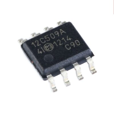
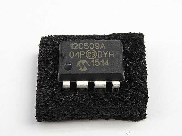
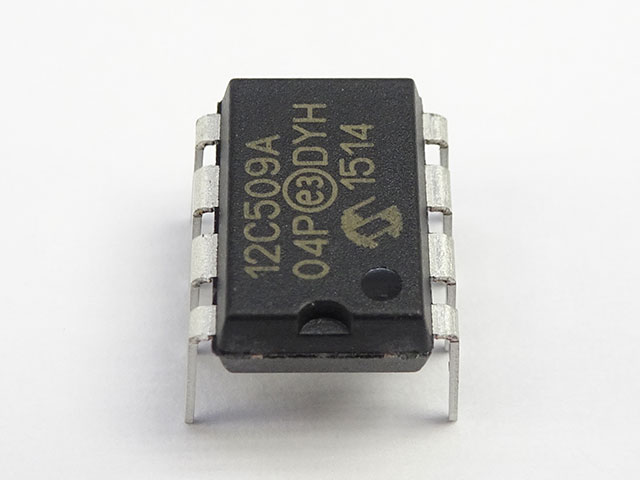
When clients need to Copy IC PIC12C509A Binary, they often face the challenge of dealing with a protected and deeply embedded 8-bit microcontroller widely used in industrial controls, small consumer devices, automotive sensors, smart tools, and custom electronic modules. The PIC12C509A’s compact design and secured memory structure make it reliable for manufacturers—but difficult for anyone who needs to retrieve, clone, or duplicate the original program or firmware stored inside it.
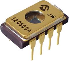
Our engineering team specializes in helping customers attack, break, and technically hack highly encrypted and locked PIC12C509A devices. Through controlled decapsulation, advanced micro-probing, and non-destructive analysis, we can decode and extract the binary, heximal, or source code-level data from the internal flash, EEPROM, or program memory. This allows us to rebuild the original file, archive, or program structure even when the chip’s protective mechanisms are fully enabled.
Copy IC PIC12C509A Binary content after unlock mcu pic12c509a flash and eeprom memory, extract program and data from microcontroller pic12c509a memory in the format of heximal;
PIC12C5XX memory is organized into program memory and data memory. For devICes with more than 512 bytes of program memory, a paging scheme is used.
Program memory pages are accessed using one STATUS register bit. For the PIC12C509, PIC12C509A, PICCR509A and PIC12CE519 with a data memory register file of more than 32 registers, a banking scheme is used. Data memory banks are accessed using the File Select Register (FSR) when break mcu pic10f200 memory.
The PIC12C5XX devICes have a 12-bit Program Counter (PC) capable of addressing a 2K x 12 program memory space. Only the first 512 x 12 (0000h-01FFh) for the PIC12C508, PIC12C508A and PIC12CE518 and 1K x 12 (0000h-03FFh) for the PIC12C509, PIC12C509A, PIC12CR509A, and PIC12CE519 are physICally implemented.
Refer to Figure 4-1. Accessing a location above these boundaries will cause a wrap around within the first 512 x 12 space (PIC12C508, PIC12C508A and PIC12CE518) or 1K x 12 space (PIC12C509, PIC12C509A, PIC12CR509A and PIC12CE519). The effective reset vector is at 000h, (see Figure 4-1). Location 01FFh (PIC12C508, PIC12C508A and PIC12CE518) or location 03FFh (PIC12C509, PIC12C509A, PIC12CR509A and PIC12CE519) contains the internal clock oscillator calibration value. This value should never be overwritten when break microcontroller pic16f886 software memory.
As a program instruction is executed, the Program Counter (PC) will contain the address of the next program instruction to be executed. The PC value is increased by one every instruction cycle, unless an instruction changes the PC.
For a GOTO instruction, bits 8:0 of the PC are provided by the GOTO instruction word. The PC Latch (PCL) is mapped to PC<7:0>. Bit 5 of the STATUS register provides page information to bit 9 of the PC (Figure 4- 8).For a CALL instruction, or any instruction where the PCL is the destination before Copy IC, bits 7:0 of the PC again are provided by the instruction word. However, PC<8> does not come from the instruction word, but is always cleared (Figure 4-8).
Instructions where the PCL is the destination, or Modify PCL instructions, include MOVWF PC, ADDWF PC, and BSF PC,5. The Program Counter is set upon a RESET, whICh means that the PC addresses the last location in the last page i.e., the oscillator calibration instruction. After executing MOVLW XX, the PC will roll over to location 00h, and begin executing user code.
The STATUS register page preselect bits are cleared upon a RESET, whICh means that page 0 is pre-selected. Therefore, upon a RESET, a GOTO instruction will automatICally cause the program to jump to page 0 until the value of the page bits is altered.
Why Clients Need This Service
Manufacturers and repair centers often require binary duplication for:
- Rebuilding obsolete or discontinued products
- Restoring damaged units when no backup exists
- Ensuring compatibility across cloned or redesigned PCB modules
- Migrating legacy firmware into newer embedded platforms
- Conducting failure analysis or system re-engineering
By enabling accurate firmware recovery, we help customers extend product life cycles, reduce downtime, and maintain operational continuity.
Difficulties & Why Expertise Matters
The PIC12C509A features strong protective code-security fuses, making direct extraction impossible through standard tools. Micro-level silicon analysis, timing-based fault techniques, and detailed memory reconstruction are required, and only an experienced specialist team can perform the process reliably without damaging the chip.
Your Trusted Technical Partner
Our service delivers fast, accurate, and confidential PIC12C509A binary extraction with full technical support. Whether your goal is cloning, duplicating, or simply retrieving critical embedded data, we provide a safe, professional solution tailored to demanding industrial requirements.