 Break Microcontroller ATmega324PA Binary
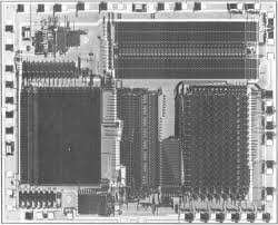
Break Microcontroller ATmega324PA flash memory and extract MCU binary out from its embedded memory, the cloned ATmega324PA processor can be made through this process;
The device can operate its Timer/Counter2 from an external 32.768 kHz watch crystal or a external clock source. See Figure 22 on page 41 for crystal connection. Applying an external clock source to TOSC1 requires EXCLK in the ASSR Register written to logic one. See “Asynchronous operation of the Timer/Counter” on page 189 for further description on selecting external clock as input instead of a 32 kHz crystal.
The ATMEAG324PA has a system clock prescaler, and the system clock can be divided by setting the “Clock Prescale Register – CLKPR” on page 49. This feature can be used to decrease the system clock frequency and the power consumption when the requirement for processing power is low.
This can be used with all clock source options, and it will affect the clock frequency of the CPU and all synchronous peripherals. clkI/O, clkADC, clkCPU, and clkFLASH are divided by a factor after copy Microcontroller atmega8l hex.
When switching between prescaler settings, the System Clock Prescaler ensures that no glitches occurs in the clock system. It also ensures that no intermediate frequency is higher than neither the clock frequency corresponding to the previous setting, nor the clock frequency corresponding to the new setting.
The ripple counter that implements the prescaler runs at the frequency of the undivided clock, which may be faster than the CPU’s clock frequency. Hence, it is not possible to determine the state of the prescaler – even if it were readable, and the exact time it takes to switch from one clock division to the other cannot be exactly predicted. From the time the CLKPS values are written, it takes between T1 + T2 and T1 + 2 * T2 before the new clock frequency is active. In this interval, 2 active clock edges are produced. Here, T1 is the previous clock period, and T2 is the period corresponding to the new prescaler setting if recover Microcontroller stm32f107rct8 code.
To avoid unintentional changes of clock frequency, a special write procedure must be followed to change the CLKPS bits:
Write the Clock Prescaler Change Enable (CLKPCE) bit to one and all other bits in CLKPR to zero.
Within four cycles, write the desired value to CLKPS while writing a zero to CLKPCE.
Interrupts must be disabled when changing prescaler setting to make sure the write procedure is not interrupted.
The CLKPCE bit must be written to logic one to enable change of the CLKPS bits. The CLKPCE bit is only updated when the other bits in CLKPR are simultaneously written to zero. CLKPCE is cleared by hardware four cycles after it is written or when CLKPS bits are written. Rewriting the CLKPCE bit within this time-out period does neither extend the time-out period, nor clear the CLKPCE bit.