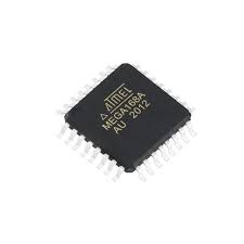
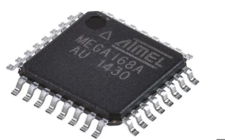
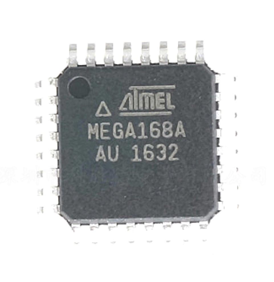
 Break MCU ATmega168A Flash
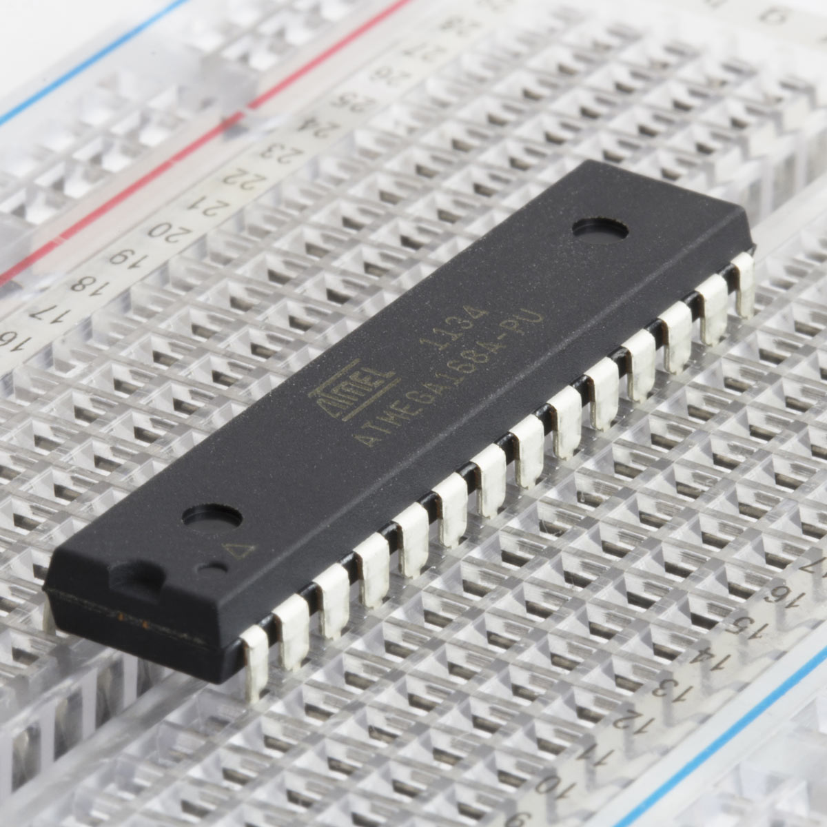
Breaking MCU ATmega168A flash involves cracking the encrypted and locked firmware to access the program and source code embedded within its secured flash memory and EEPROM memory. This protective microcontroller (MCU) is designed to safeguard its binary and heximal data against unauthorized access. However, reverse engineering techniques can be employed to decode and unlock its secured firmware for legitimate purposes such as system restoration or hardware cloning.
Quebrar o flash MCU ATmega168A envolve quebrar o firmware criptografado e bloqueado para acessar o programa e o código-fonte embutidos em sua memória flash segura e memória EEPROM. Este microcontrolador de proteção (MCU) é projetado para proteger seus dados binários e hexagonais contra acesso não autorizado. No entanto, técnicas de engenharia reversa podem ser empregadas para decodificar e desbloquear seu firmware seguro para fins legítimos, como restauração do sistema ou clonagem de hardware.
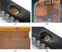
The process requires an in-depth understanding of the microprocessor’s architecture to bypass security features and retrieve the embedded software. Advanced tools are used to extract and decode the encrypted data stored in the flash memory. Once unlocked, the firmware can be restored to its original functionality or cloned for replication in similar systems.
While breaking the ATmega168A’s flash provides a solution for restoring or replicating old or damaged microcomputers, it must be performed within ethical and legal boundaries to ensure intellectual property rights are respected.
Break MCU ATmega168A Flash
Most of the instructions operating on the Register File have direct access to all registers, and most of them are single cycle instructions. Each register is also assigned a data memory address, mapping them directly into the first 32 locations of the user Data Space. Although not being physically implemented as SRAM locations, this memory organization provides great flexibility in access of the registers which is useful for Break MCU ATmega168A Flash, as the X-, Y- and Z-pointer registers can be set to index any register in the file. The registers R26..R31 have some added functions to their general purpose usage.
These registers are 16-bit address pointers for indirect addressing of the data space. The Stack is mainly used for storing temporary data, for storing local variables and for storing return addresses after interrupts and subroutine calls.
MCU ATmega168A flaşını kırmak, güvenli flaş belleği ve EEPROM belleğinde gömülü programa ve kaynak koduna erişmek için şifrelenmiş ve kilitlenmiş aygıt yazılımını kırmayı içerir. Bu koruyucu mikrodenetleyici (MCU), ikili ve heksimal verilerini yetkisiz erişime karşı korumak için tasarlanmıştır. Ancak, tersine mühendislik teknikleri, sistem geri yükleme veya donanım klonlama gibi meşru amaçlar için güvenli aygıt yazılımını çözmek ve kilidini açmak için kullanılabilir.
The Stack Pointer Register always points to the top of the Stack. Note that the Stack is implemented as growing from higher memory locations to lower memory locations. This implies that a Stack PUSH command decreases the Stack Pointer by Hack IC firmware. The Stack Pointer points to the data SRAM Stack area where the Subroutine and Interrupt Stacks are located. This Stack space in the data SRAM must be defined by the program before any subroutine calls are executed or interrupts are enabled.
The Stack Pointer must be set to point above 0x0100, preferably RAMEND. The Stack Pointer is decremented by one when data is pushed onto the Stack with the PUSH instruction, and it is decremented by two when the return address is pushed onto the Stack with subroutine call or interrupt.
recover embedded firmware from atmega168a mcu flash memory
The Stack Pointer is incremented by one when data is popped from the Stack with the POP instruction, and it is incremented by two when data is popped from the Stack with return from subroutine RET or return from interrupt RETI.
The AVR Stack Pointer is implemented as two 8-bit registers in the I/O space. The number of bits actually used is implementation dependent. Note that the data space in some implementations of the AVR architecture is so small that only SPL is needed. In this case, the SPH Register will not be present after Extract MCU Firmware.
This section describes the general access timing concepts for instruction execution. The AVR CPU is driven by the CPU clock clkCPU, directly generated from the selected clock source for the MCU Cracking. No internal clock division is used.
Figure 5-4 shows the parallel instruction fetches and instruction executions enabled by the Harvard architecture and the fast-access Register File concept. This is the basic pipelining concept to obtain up to 1 MIPS per MHz with the corresponding unique results for functions per cost, functions per clocks, and functions per power-unit.
break ATMEGA168A secured microprocessor fuse bit and readout embedded program from flash memory and data from eeprom memory
The AVR provides several different interrupt sources. These interrupts and the separate Reset Vector each have a separate program vector in the program memory space. All interrupts are assigned individual enable bits which must be written logic one together with the Global Interrupt Enable bit in the Status Register in order to enable the interruption in the process of Break MCU ATmega168A Flash. Depending on the Program Counter value, interrupts may be automatically disabled when Boot Lock bits BLB02 or BLB12 are programmed. This feature improves software security. See the section ”Memory Programming” on page 285 for details.
Взлом флэш-памяти MCU ATmega168A включает взлом зашифрованной и заблокированной прошивки для доступа к программе и исходному коду, встроенному в защищенную флэш-память и память EEPROM. Этот защитный микроконтроллер (MCU) предназначен для защиты своих двоичных и шестнадцатеричных данных от несанкционированного доступа. Однако методы обратного проектирования могут быть использованы для декодирования и разблокировки его защищенной прошивки в законных целях, таких как восстановление системы или клонирование оборудования.