 Break MCU ATmega128PA Heximal
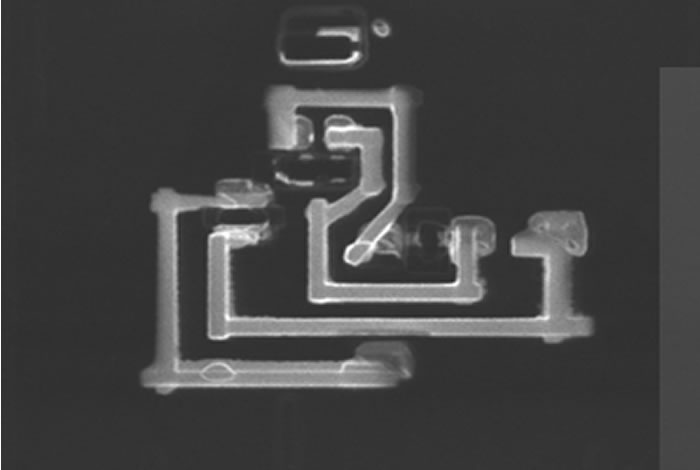
Break MCU ATmega128APA flash memory and readout chip ATmega128PA content inside it in the format of Heximal, the code can be reprogrammed to new ATmega128PA microcontroller for cloning;
OC1A/PCINT5, Bit 5
OC1A, Output Compare Match A output: The PB5 pin can serve as an external output for the Timer/Counter1 Output Compare A. The pin has to be configured as an output (DDB5 set (one)) to serve this function. The OC1A pin is also the output pin for the PWM mode timer function.
PCINT5, Pin Change Interrupt source 5: The PB7 pin can serve as an external interrupt source.
OC2A/PCINT4, Bit 4
OC2A, Output Compare Match output: The PB4 pin can serve as an external output for the Timer/Counter2 Output Compare. The pin has to be configured as an output (DDB4 set (one)) to serve this function. The OC2A pin is also the output pin for the PWM mode timer function when recover mcu pic16c554 software.
PCINT4, Pin Change Interrupt source 4: The PB7 pin can serve as an external interrupt source.
MISO/PCINT3 – Port B, Bit 3
MISO: Master Data input, Slave Data output pin for SPI channel. When the SPI is enabled as a master, this pin is configured as an input regardless of the setting of DDB3. When the SPI is enabled as a slave, the data direction of this pin is controlled by DDB3. When the pin is forced to be an input, the pull-up can still be controlled by the PORTB3 bit.
PCINT3, Pin Change Interrupt source 3: The PB7 pin can serve as an external interrupt source when Break MCU heximal.
MOSI/PCINT2 – Port B, Bit 2
MOSI: SPI Master Data output, Slave Data input for SPI channel. When the SPI is enabled as a slave, this pin is configured as an input regardless of the setting of DDB2. When the SPI is enabled as a master, the data direction of this pin is controlled by DDB2. When the pin is forced to be an input, the pull-up can still be controlled by the PORTB2 bit.
PCINT2, Pin Change Interrupt source 2: The PB7 pin can serve as an external interrupt source.
SCK/PCINT1 – Port B, Bit 1
SCK: Master Clock output, Slave Clock input pin for SPI channel. When the SPI is enabled as a slave, this pin is configured as an input regardless of the setting of DDB1. When the SPI0 is enabled as a master, the data direction of this pin is controlled by DDB1. When the pin is forced to be an input, the pull-up can still be controlled by the PORTB1 bit.
PCINT1, Pin Change Interrupt source 1: The PB7 pin can serve as an external interrupt source.