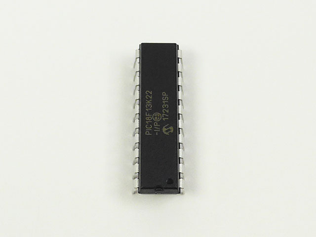
 Attack Microchip PIC18F13K22 Microcontroller Flash Memory
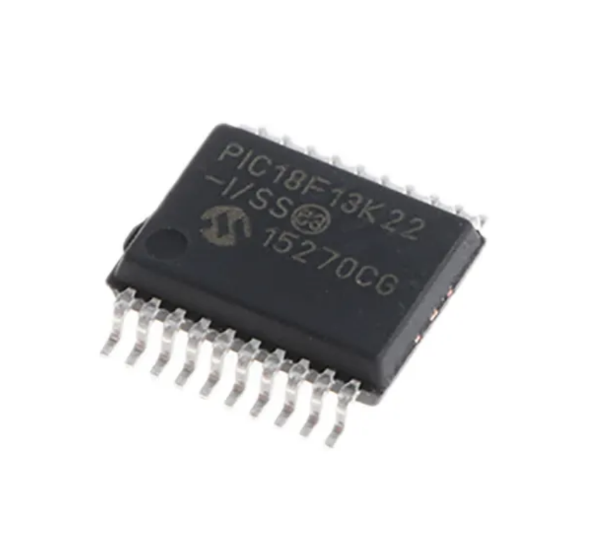
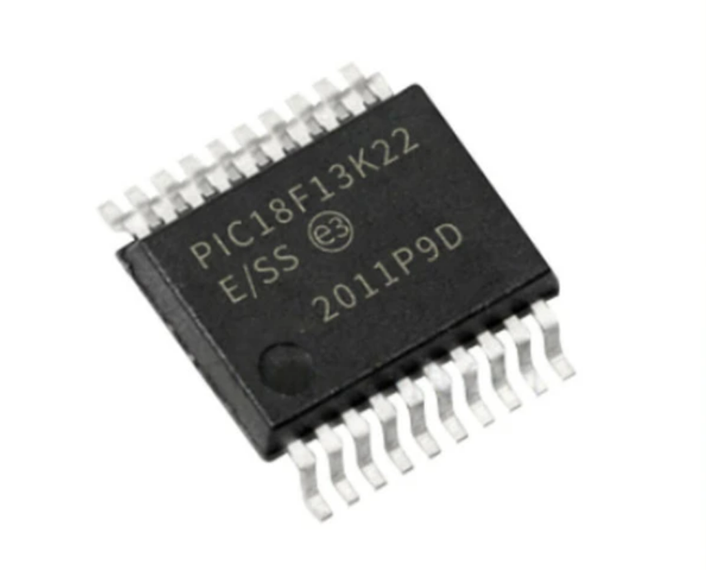
Attack Microchip PIC18F13K22 Microcontroller Flash Memory and extract the embedded firmware from microprocessor, the new MCU PIC18F13K22 will be served as MCU cloning units;

This family offers the advantages of all PIC18 microcontrollers – namely, high computational performance with the addition of high-endurance, Flash program memory. On top of these features, the PIC18F13K22 family introduces design enhancements that make these microcontrollers a logical choice for many high-performance, power sensitive applications.
All of the devices in the PIC18F1XK22/LF1XK22 family incorporate a range of features that can significantly reduce power consumption during operation. Key items include:
माइक्रोचिप सुरक्षित PIC18F13K22 माइक्रोकंट्रोलर फ्लैश प्रोग्राम मेमोरी और ईप्रोम डेटा मेमोरी सुरक्षा पर हमला करें, और एन्क्रिप्टेड माइक्रोप्रोसेसर PIC18F13K22 से बाइनरी फ़ाइल या हेक्सिमल सॉफ़्टवेयर के प्रारूप में एम्बेडेड फ़र्मवेयर निकालें, प्रतिकृति के लिए नए MCU माइक्रोचिप PIC18F13K22 में स्रोत कोड की प्रतिलिपि बनाएँ;
- Multiple Idle Modes: The controller can also run with its CPU core disabled but the peripherals still active. In these states, power consumption can be reduced even further, to as little as 4% of normal operation requirements.
- On-the-fly Mode Switching: The
power-managed modes are invoked by user code during operation, allowing the user to incorporate power-saving ideas into their application’s software design to be used for attacking microcontroller pic18f66k90 memory.Low Consumption in Key Modules: The power requirements for both Timer1 and the Watchdog Timer are minimized. See Section 25.0 “Electrical Specifications” for values.
All of the devices in the PIC18F1XK22/LF1XK22 family offer ten different oscillator options, allowing users a wide range of choices in developing application hardware. These include:
- Four Crystal modes, using crystals or ceramic resonators
- External Clock modes, offering the option of using two pins (oscillator input and a divide-by-4 clock output) or one pin (oscillator input, with the sec- ond pin reassigned as general I/O)
- External RC Oscillator modes with the same pin options as the External Clock modes
- An internal oscillator block which contains a 16 MHz HFINTOSC oscillator and a 31 kHz LFINTOSC oscillator which together provide 8
atacar la memoria flash del microcontrolador PIC18F13K22 asegurada por Microchip y la protección de la memoria de datos eeprom, y extraer el firmware integrado en formato de archivo binario o software heximal del microprocesador cifrado PIC18F13K22, copiar el código fuente en el nuevo microchip PIC18F13K22 de MCU para su replicación;
user selectable clock frequencies, from 31 kHz to 16 MHz. This option frees the two oscillator pins for use as additional general purpose I/O.
- A Phase Lock Loop (PLL) frequency multiplier, available to both the high-speed crystal and inter- nal oscillator modes, which allows clock speeds of up to 64 MHz. Used with the internal oscillator, the PLL gives users a complete selection of clock speeds, from 31 kHz to 32 MHz – all without using an external crystal or clock circuit.
Besides its availability as a clock source, the internal oscillator block provides a stable reference source that gives the family additional features for robust operation:
- Fail-Safe Clock Monitor: This option constantly monitors the main clock source against a refer- ence signal provided by the LFINTOSC. If a clock failure occurs, the controller is switched to the internal oscillator block, allowing for continued operation or a safe application shutdown.
attaccare la memoria flash del programma microcontroller PIC18F13K22 protetta da Microchip e la protezione della memoria dati eeprom ed estrarre il firmware incorporato nel formato di file binario o software esimale dal microprocessore crittografato PIC18F13K22, copiare il codice sorgente nel nuovo microchip MCU PIC18F13K22 per la replica;
Two-Speed Start-up: This option allows the internal oscillator to serve as the clock source from Power-on Reset, or wake-up from Sleep mode, until the primary clock source is available.