Archive for the ‘Recover MCU’ Category
 Decode SPC560P54L5 secured binary firmware
 February 24th, 2021 |
 Author:
The phrase decode SPC560P54L5 secured binary firmware covers several different deliverables – a program file, a labelled image or simply an identification report. This page separates those outcomes for the SPC560P54L5. SPC560P54L5 is STMicroelectronics’ SPC56 P-line chassis MCU: 768 Kbytes of code flash and 64 Kbytes of SRAM.
An honest answer to decode SPC560P54L5 secured binary firmware
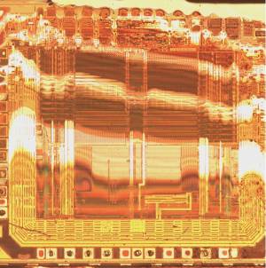
The SPC560P54L5 belongs to STMicroelectronics’ SPC56 P line, a 32-bit Power Architecture family for chassis and safety applications that traces its origin to the ST-Freescale automotive MCU programme. The device carries 768 Kbytes of code flash, 64 Kbytes of data flash for EEPROM emulation and 64 Kbytes of SRAM, all protected by ECC. Safety features include a software watchdog with a pseudo-random servicing sequence, a fault collection and control unit and a safe mode. The term heximal appears throughout legacy service notes, but what an engineer actually needs is a labelled program and data file set.
Flash endurance and image integrity
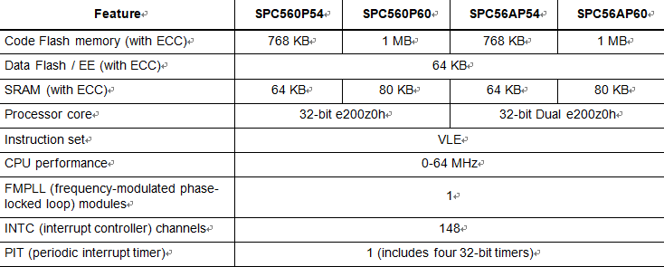
Program storage is up to 1024 Kbytes of on-chip code flash with an erase/program controller, and the 54 member is fitted with 768 Kbytes. A separate 64 Kbyte data flash block supports EEPROM emulation, and the SRAM is 64 Kbytes with ECC. ECC on both flash and SRAM means a diagnostic report should include the error-status log. The two flash arrays have distinct erase geometries, so a captured image must label code and data regions separately. The surrounding microcontroller cross-reference is documented in SPC56AP54L5 flash documentation.
Why a peripheral is not a backdoor
| Item | What the data sheet states |
|---|---|
| Part | e200z0h at 64 MHz / 768 KB code Flash / 64 KB SRAM / ST SPC56 P-line |
| Core | e200z0h, 32-bit Power Architecture VLE, 64 MHz, dual-issue, 3.0 or 5.0 V I/O |
| Memory | 768 KB code Flash / 64 KB data Flash / 64 KB SRAM / 64 MHz / LQFP144 |
| Program memory | up to 1024 KB code Flash with ECC plus 64 KB data Flash for EEPROM emulation |
| RAM | 64 KB on-chip SRAM with ECC |
| Package | LQFP144, -40 to 105 or 125 C, tape-and-reel |
| Boot interface | Boot Assist Module with CAN/UART loader; Nexus L2+ debug interface |
The device implements a register protection scheme and a censorship state, and with protection set a debug probe cannot read the flash or SRAM while identification remains available. The Boot Assist Module and the CAN/UART loader write new code; they do not read a protected image back out. For a protected sample the achievable deliverable is a documented identification and an archive comparison. A comparable recovery note is SPC5602PEF0MLH6 flash documentation.
ADC and timer configuration
Communication includes two FlexCAN interfaces, a safety port based on FlexCAN, two LINFlex modules, five DSPI modules and a FlexRay controller with dual or single channel operation up to 10 Mbit per second. Two eDMA controllers with sixteen channels, two eTimer units, a cross-trigger unit and a 10-bit ADC with 27 input channels handle control and conversion. A documentation record should capture the FlexRay configuration, the CAN filters and the safety port settings. Protective lock bits, an encrypted data region and a secured boot configuration are three separate concepts that an identification report must distinguish. Further reading on adjacent SPC56 and MCU boards: SPC5603CK0CLL6 flash documentation.
Marking, schematic and supply checks
The P54 member is published in a 144-pin LQFP body with -40 to 105 or -40 to 125 degree grades, identified by the BEAAR and CEAAR endings. The FlexRay configuration is central to a chassis design and belongs in any service note. The 144-pin package exposes 80 GPIO plus 26 GPI, so firmware written for it will not map onto a 100-pin sibling. A single 3.3 V or 5 V supply is used for I/O and ADC, with the core regulated on chip. The wider NXP, ST and general MCU material is linked here: Arm microcontroller stm32f207igt6 Flash firmware recovery.
Technical findings, not a bypass
The SPC56 P line is the ST-built branch of the same Power Architecture automotive family as the NXP MPC56xx parts, so a board may carry either brand marking. Pin compatibility across the P54 and P60 capacities means a device can be swapped until the flash budget is exceeded. Flash size, safety grade and package are the three facts that identify the member. Our engagement begins with a written identification record: package marking, ordering code, device identification, clock source, supply rails and safety configuration, followed by an archive comparison. We disclose the mass-erase consequence before any destructive step, work under NDA for the owner or an appointed repair partner, and never quote a readout that depends on defeating the protection state. Related device notes on this site cover the wider Power Architecture MCU family: Arm microprocessor stm32f071r8 Flash code restoration.
If you need to decode SPC560P54L5 secured binary firmware, the practical first step is a written identification report: package marking, ordering code, device identification, clock source and supply rails, followed by a comparison with any build archive you hold. Our engineers document those findings, explain whether a clean read is possible, and state the mass-erase limit before any destructive work is authorised. We work under NDA for legitimate owners and their appointed repair partners, and we do not quote a readout that depends on suppressing a protection state.
 Posted in

Retrieve SPC5604PGF1VLQ6 protected source code
Most retrieve SPC5604PGF1VLQ6 protected source code enquiries can be resolved on paper: read the data sheet, note the configuration and compare the owner’s release archive. The SPC5604PGF1VLQ6 is a good example, because its protection behaviour is documented in plain terms. The G in PGF1 marks the FlexRay-capable P-line member with 512 Kbytes of flash and 40 Kbytes of RAM.
Clarifying retrieve SPC5604PGF1VLQ6 protected source code for an automotive board
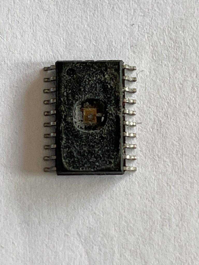
The P-line raises the e200z0h core to 64 MHz and pairs it with a larger SRAM budget than the D parts, which is why these devices appear in body, chassis and safety-related controllers. The core executes Power Architecture VLE code and remains single-issue, and a crossbar switch connects it to flash and to the peripheral bridges. The 64 MHz e200z0h core and the FlexRay option define this ordering group. An unlocked microcontroller yields a clean software image; a locked chip yields documentation and a comparison exercise instead.
Data flash and its emulation role
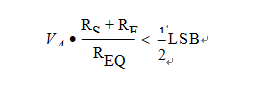
Code flash is 256 Kbytes on the 5602 and 512 Kbytes on the 5604, with 20 or 40 Kbytes of SRAM and a data flash region for EEPROM emulation. ECC protects the code flash and the SRAM, and the error correction status module records corrected and uncorrectable events that belong in any diagnostic note. The 256 / 512 KB Flash / 20 / 40 KB SRAM / 64 MHz specification is the ordering reference for the P line. For background on a neighbouring automotive controller, see SPC560P54L5 flash documentation.
Protect, erase, or document
| Item | What the data sheet states |
|---|---|
| Part | e200z0h at 64 MHz / 512 KB code Flash / 40 KB SRAM / FlexRay / LQFP144 |
| Core | e200z0h, 32-bit Power Architecture VLE, 64 MHz, single core, 3.0-5.5 V |
| Memory | 256 / 512 KB Flash / 20 / 40 KB SRAM / 64 MHz / FlexRay on G members |
| Program memory | on-chip code Flash with ECC plus a data Flash block for EEPROM emulation |
| RAM | 20 KB (5602P) or 40 KB (5604P) on-chip SRAM |
| Package | LQFP64 / LQFP100 / LQFP144, -40 to 105 or 125 C, tray or reel |
| Boot interface | Boot Assist Module (BAM) plus a CAN/UART serial bootstrap loader |
Censorship is a configuration state held in the flash, and with it set a debug probe cannot read the flash or SRAM contents even though the device still identifies itself. A mass erase clears the state and erases the application in the same operation. ECC on both flash and SRAM means an error-status log is part of a defensible diagnostic record. The FlexRay controller, the eDMA engine and the safety monitor are legitimate peripherals, not a service backdoor. The surrounding microcontroller cross-reference is documented in SPC5601PEF flash documentation.
Baud rates, clocks and PLL settings
The peripheral inventory includes multiple FlexCAN channels, LINFlex UARTs, DSPI modules, a 10 or 12-bit ADC with cross triggering, eDMA and a software watchdog. G-suffix members add a FlexRay controller with dual or single channel operation and up to 10 Mbit per second, which is the feature that separates them in a chassis design. Timers include a system timer module, periodic interrupt timers and a real-time counter, while the fault collection unit drives safe-state behaviour. A source code archive, a compiled binary and a raw heximal each answer a different question about the same microcontroller. A comparable recovery note is SPC5603BK0CLQ4R flash documentation.
Tray versus reel packing codes
Ordering codes select 64, 100 or 144-pin LQFP bodies as well as temperature grade and packing. The larger body exposes more I/O and ADC channels, so a schematic is not enough to prove which package is fitted. A trailing R means tape-and-reel packing and does not change the flash or the protection behaviour. Further reading on adjacent SPC56 and MCU boards: Arm microcontroller stm32f101c4 locked firmware recovery.
Written scope and NDA practice
The P-line shares the e200z0h core with the D, B and C lines but runs faster and carries more RAM and safety peripherals. A 64-pin body has fewer ADC channels than the 144-pin part, so a captured image may reference pins that do not exist. Several members are pin-compatible, so a board can accept a smaller flash part until the application overruns it. Flash size, SRAM size and the presence of FlexRay are the three facts that identify the fitted member. A written scope covers marking, ordering code, device identification, clock source, supply rails and the safety configuration, then compares the owner’s release archive with what the fitted device reports. With censorship disabled we can return labelled code and data flash images; with it enabled we supply documentation and an archive comparison. The wider NXP, ST and general MCU material is linked here: Arm microcontroller stm32f205rg Flash code recovery.
Owners considering retrieve SPC5604PGF1VLQ6 protected source code should expect a technical deliverable first: a datasheet-based identification record, a labelled image where the protection state permits one, and a clear written statement where it does not. We explain that a mass erase removes the firmware together with the protection, require written authorisation before any destructive step, and never price a service that depends on defeating the protection state. That boundary is what keeps a recovered program file usable as evidence years later.
Clone SPC5604BK0CLQ6 locked memory program
A technician asked to clone SPC5604BK0CLQ6 locked memory program should begin with the package marking and the supply rails. On the SPC5604BK0CLQ6 several ordering codes share one core, so the suffix is the first thing worth recording. This 144-pin B-line part carries 512 Kbytes of flash, 32 Kbytes of SRAM and a 64 MHz e200z0h core.
Where clone SPC5604BK0CLQ6 locked memory program meets the data sheet
The B-line members are the mid-capacity MPC56xx devices, pairing 384 or 512 Kbytes of code flash with 28 or 32 Kbytes of SRAM on the e200z0h core. The 64 Kbyte data flash is the largest in this group, so its emulation geometry belongs in the archive manifest. A crossbar switch and an eDMA controller keep the flash and the communication bridges fed without constant core intervention. Standard interfaces include FlexCAN, LINFlex, DSPI, a 12-bit ADC and I2C on the larger bodies, which is why these parts are common in body and industrial control. Retrieving configuration data from a secured MCU is a separate task from reconstructing the program that once used it.
Separating code and data flash
Code flash is 384 Kbytes on the 5603 and 512 Kbytes on the 5604, and both carry a 64 Kbyte data flash block for EEPROM emulation. Because the two arrays have different sector sizes, a firmware archive must label code and data separately; a merged heximal loses the emulation geometry. The 384 / 512 KB Flash / 28 / 32 KB SRAM / 64 KB data Flash table identifies this line. Related device notes on this site cover the wider Power Architecture MCU family: SPC5604PGF1VLQ6 flash documentation.
Identification on a protected device
| Item | What the data sheet states |
|---|---|
| Part | e200z0h at 64 MHz / 512 KB code Flash / 32 KB SRAM / LQFP144 |
| Core | e200z0h, 32-bit Power Architecture VLE, 48 or 64 MHz, 3.0-5.5 V |
| Memory | 384 / 512 KB Flash / 28 / 32 KB SRAM / 64 KB data Flash / 48-64 MHz |
| Program memory | on-chip code Flash with ECC plus 64 KB data Flash for EEPROM emulation |
| RAM | 28 KB (5603B, 48 MHz) or 32 KB (5604B, 64 MHz) SRAM |
| Package | LQFP100 / LQFP144, -40 to 85 C, tray or tape-and-reel |
| Boot interface | Boot Assist Module (BAM) and CAN/UART serial bootstrap loader |
Protection is a censorship state in the flash configuration, not a cryptographic engine. With censorship set, a debug interface cannot read the flash or SRAM while the device identification remains visible. The ADC, the CAN controllers and the eDMA engine are application features with no alternate readout role. For background on a neighbouring automotive controller, see SPC5601DF1MLL4 flash documentation.
The timer, watchdog and port blocks
The B-line peripheral set includes FlexCAN, I2C, LINFlex, DSPI, a 12-bit ADC with up to 36 channels and multiple timer modules. A phase-locked loop generates the core and bus clocks from a crystal or an internal oscillator, and a watchdog supervises execution. A 144-pin body exposes more ADC channels than a 100-pin part, changing the channel assignment in firmware. A reconstructed program record should note the ADC channel assignment, the CAN acceptance filters and the eTimer configuration. An attack on the security field is explicitly out of scope; what remains is documenting the microprocessor, its flash geometry and its program file. The surrounding microcontroller cross-reference is documented in SPC5602DF1VLH4R flash documentation.
Footprints, rails and test points
Ordering codes distinguish a 100-pin from a 144-pin LQFP and select temperature grade and packing; the CLQ4R and CLQ6 endings mark those bodies. The 144-pin part exposes substantially more I/O and ADC inputs, so firmware written for it cannot be assumed to fit the 100-pin device. The marked ordering code is the only dependable way to separate a 384 Kbyte from a 512 Kbyte part on an unlabelled board. A comparable recovery note is Arm microcontroller stm32f071v8 source code decryption.
Deliverables for a legitimate owner
The B line sits between the smaller D parts and the faster P parts in the MPC56xx range, sharing the core but not the memory budget. Pin compatibility across capacities means a board can boot with the wrong flash size until the linker map overruns. The C-line devices share similar flash sizes but differ in SRAM and package, so the family name alone is not enough. Our written handover starts with marking, ordering code, identification, clock source and supply rails, then compares the owner’s archived build with the fitted device. The 48 to 64 MHz clock difference between the two capacities affects timing loops written against the core. We state the mass-erase consequence before any destructive step, work under NDA for the owner or an appointed repair partner, and never quote a readout that depends on defeating the protection state. Further reading on adjacent SPC56 and MCU boards: Arm microcontroller stm32f100r6 secured Flash breaking.
To discuss clone SPC5604BK0CLQ6 locked memory program for a specific module, send the marking, the schematic if available and the reason the original build output is no longer accessible. We return a feasibility note that separates what the silicon exposes from what would require destroying the application, and we only proceed after the owner confirms the scope in writing. Automotive Power Architecture controllers are our regular work, and the handover is a documented file set rather than an undocumented promise about a locked chip.
Decapsulate SPC5603CK0CLL6 secured integrated circuit code
Before you decapsulate SPC5603CK0CLL6 secured integrated circuit code, identify which SPC56 line is fitted. The SPC5603CK0CLL6 has a specific flash and SRAM budget, and those two numbers determine the rest of the workflow. The CK0CLL6 code is the 100-pin, 64 MHz C-line device pairing 384 Kbytes of flash with 40 Kbytes of RAM.
Before attempting to decapsulate SPC5603CK0CLL6 secured integrated circuit code
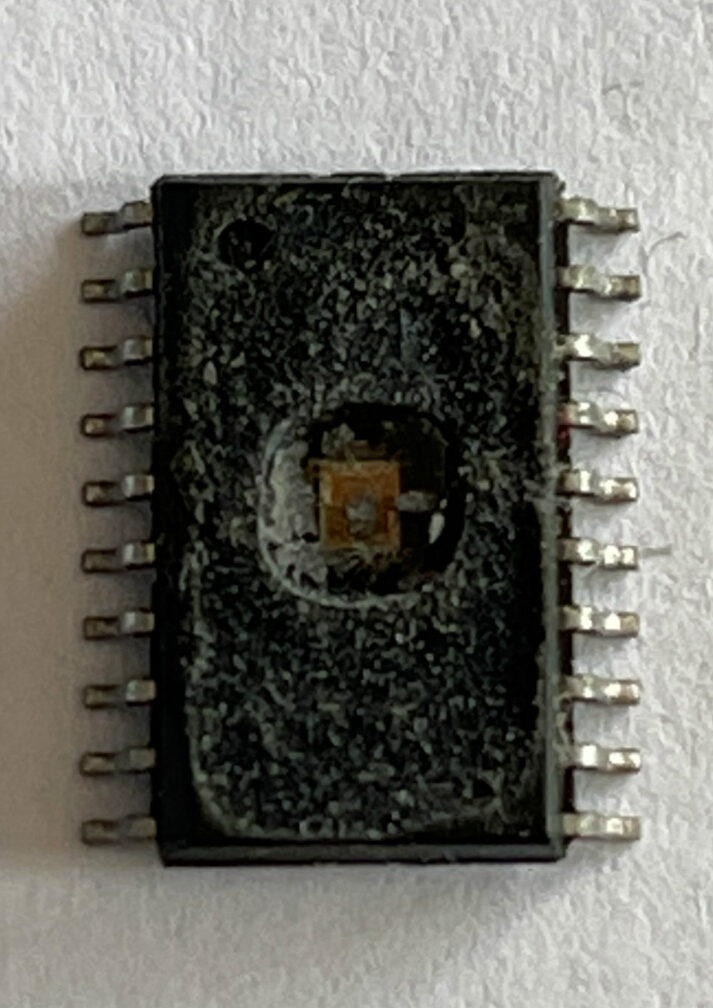
The C-line member pairs 384 Kbytes of code flash with a comparatively large 40 Kbyte SRAM on a 64 MHz e200z0h core. That combination suits body applications with a substantial runtime data footprint, and the part executes the compact VLE form of the Power Architecture instruction set. The 40 Kbyte SRAM on a 100-pin body is the feature that identifies this member. An encrypted binary is not the same thing as a protected flash array, and no peripheral here serves as a readout engine.
Code, data and configuration regions
Code memory is 384 Kbytes of flash, data memory is 40 Kbytes of SRAM, and a 64 Kbyte data flash block supports EEPROM emulation. The 100-pin body limits ADC channels relative to the 144-pin siblings in the same capacity range. The code and data flash arrays have different erase geometries, so an archive must record them as separate images. ECC covers both the code flash and the SRAM, and the error correction status module reports corrected events that matter in a safety-related diagnosis. The wider NXP, ST and general MCU material is linked here: SPC5604BK0CLQ6 flash documentation.
What the identification registers report
| Item | What the data sheet states |
|---|---|
| Part | e200z0h at 64 MHz / 384 KB code Flash / 40 KB SRAM / LQFP100 |
| Core | e200z0h, 32-bit Power Architecture VLE, 64 MHz, 3.0-5.5 V |
| Memory | 384 KB Flash / 40 KB SRAM / 64 KB data Flash / 64 MHz / LQFP100 |
| Program memory | on-chip code Flash with ECC plus 64 KB data Flash for EEPROM emulation |
| RAM | 40 KB on-chip SRAM with ECC |
| Package | LQFP100, -40 to 85 C, tray packing |
| Boot interface | Boot Assist Module (BAM) and CAN/UART serial bootstrap loader |
The device enforces a censorship state stored in the flash configuration; while it is set, debug reads of flash and SRAM are blocked and identification still works. A mass erase clears the state and the application together, which is why a signed build archive is the stronger evidence. The ADC, the CAN controller and the eDMA engine are normal peripherals and provide no alternate route around censorship. Related device notes on this site cover the wider Power Architecture MCU family: SPC56AP54L5 flash documentation.
Clock, CAN and safety settings
Peripherals include FlexCAN, LINFlex, DSPI, I2C, a 12-bit ADC with a cross-trigger unit and a set of 32-bit timers. The eDMA controller supports multiple channels with arbitration, and a watchdog and periodic interrupt timers handle scheduling and recovery. A firmware record should capture the CAN filters, the ADC trigger chain and the eDMA channel assignments. Retrieving data from a secured MCU, reviewing an encrypted binary or cloning a locked file all reduce to the same identification step on this family. For background on a neighbouring automotive controller, see SPC5602PEF0MLH6 flash documentation.
How the SPC5603CK0CLL6 differs from its siblings
This member is published in a 100-pin LQFP with a -40 to 85 degree range and tray packing, as the CLL6 ending indicates. The 100-pin body limits the available I/O and ADC channels compared with the 144-pin siblings in the B and P lines. The 40 Kbyte SRAM is unusually large for a 384 Kbyte member, which changes the runtime footprint assumptions in a firmware review. Decoupling with a ceramic capacitor at each supply pair and a bulk part on the rail remains standard. The surrounding microcontroller cross-reference is documented in Arm microcontroller stm32f051c4 Flash binary recovery.
Authorisation, archive and handover
Within MPC56xx the C line is close to the B line in flash size but carries more SRAM, which changes the linker script rather than the pin-out. The P line runs the same core at 64 MHz with different peripherals, so the family name alone is not identification evidence. Flash size, SRAM size and package are the three facts that separate this member. A written scope covers marking, ordering code, identification, clock source and supply rails, followed by a comparison with the owner’s build archive. When censorship is off we can hand back labelled code and data flash images; when it is on we deliver an identification and documentation package. We do not quote a readout that depends on defeating the protection state. A comparable recovery note is Arm microcontroller stm32f071c8 heximal program recovery.
Any decapsulate SPC5603CK0CLL6 secured integrated circuit code request is handled the same way on every SPC56 board: identify the fitted line, record the memory map and clock tree, then compare the customer’s archived build output with what the debug interface reports. Where the array is unprotected a labelled program file can be returned; where it is protected we supply an identification and documentation package instead. All work is scoped in writing for the owner or an authorised agent, with the erase consequence stated up front.
Break SPC5603BK0CLQ4R protected flash file
When a control module arrives with no source code, the request is often phrased as break SPC5603BK0CLQ4R protected flash file. For the SPC5603BK0CLQ4R the honest answer starts with the flash geometry and ends with a written record of what the debug interface reports. A 144-pin LQFP and the -40 to 85 degree range identify this 384 Kbyte B-line member with 28 Kbytes of SRAM.
Technical basis for break SPC5603BK0CLQ4R protected flash file
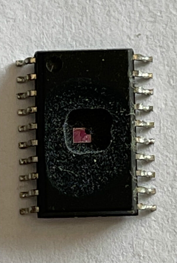
The B-line members are the mid-capacity MPC56xx devices, pairing 384 or 512 Kbytes of code flash with 28 or 32 Kbytes of SRAM on the e200z0h core. A crossbar switch and an eDMA controller keep the flash and the communication bridges fed without constant core intervention. Standard interfaces include FlexCAN, LINFlex, DSPI, a 12-bit ADC and I2C on the larger bodies, which is why these parts are common in body and industrial control. Whether the target is data, code or a complete heximal, the identification step is identical and always comes first.
The program array and its regions
Code flash is 384 Kbytes on the 5603 and 512 Kbytes on the 5604, and both carry a 64 Kbyte data flash block for EEPROM emulation. ECC tags on the code flash and the SRAM are reported through the error correction status module, which a diagnostic report should record. The 384 / 512 KB Flash / 28 / 32 KB SRAM / 64 KB data Flash table identifies this line. Further reading on adjacent SPC56 and MCU boards: SPC5603CK0CLL6 flash documentation.
The protection state and erase consequence
| Item | What the data sheet states |
|---|---|
| Part | e200z0h at 48 MHz / 384 KB code Flash / 28 KB SRAM / LQFP144 |
| Core | e200z0h, 32-bit Power Architecture VLE, 48 or 64 MHz, 3.0-5.5 V |
| Memory | 384 / 512 KB Flash / 28 / 32 KB SRAM / 64 KB data Flash / 48-64 MHz |
| Program memory | on-chip code Flash with ECC plus 64 KB data Flash for EEPROM emulation |
| RAM | 28 KB (5603B, 48 MHz) or 32 KB (5604B, 64 MHz) SRAM |
| Package | LQFP100 / LQFP144, -40 to 85 C, tray or tape-and-reel |
| Boot interface | Boot Assist Module (BAM) and CAN/UART serial bootstrap loader |
Protection is a censorship state in the flash configuration, not a cryptographic engine. A 144-pin body exposes more ADC channels than a 100-pin part, changing the channel assignment in firmware. With censorship set, a debug interface cannot read the flash or SRAM while the device identification remains visible. The ADC, the CAN controllers and the eDMA engine are application features with no alternate readout role. The wider NXP, ST and general MCU material is linked here: SPC560P54L5 flash documentation.
Peripherals that shape a firmware archive
The B-line peripheral set includes FlexCAN, I2C, LINFlex, DSPI, a 12-bit ADC with up to 36 channels and multiple timer modules. Two 16-bit eTimer units provide quadrature decoding and input capture, and a cross-trigger unit connects the ADC to the timers. A phase-locked loop generates the core and bus clocks from a crystal or an internal oscillator, and a watchdog supervises execution. Reviewing a protected part is not the same as decoding an unprotected one, and a decapsulated chip still needs the owner’s build archive before any code is reconstructed. Related device notes on this site cover the wider Power Architecture MCU family: SPC5601PEF flash documentation.
Package suffixes and board access
Ordering codes distinguish a 100-pin from a 144-pin LQFP and select temperature grade and packing; the CLQ4R and CLQ6 endings mark those bodies. Automotive decoupling with a ceramic part at each supply pair and a bulk capacitor on the rail is standard. The marked ordering code is the only dependable way to separate a 384 Kbyte from a 512 Kbyte part on an unlabelled board. For background on a neighbouring automotive controller, see Arm microcomputer stm32f072r8 readout protection breaking.
Commercial terms of the service
The B line sits between the smaller D parts and the faster P parts in the MPC56xx range, sharing the core but not the memory budget. Pin compatibility across capacities means a board can boot with the wrong flash size until the linker map overruns. The 48 to 64 MHz clock difference between the two capacities affects timing loops written against the core. Flash size, SRAM size and pin count are the three numbers to record first. Our written handover starts with marking, ordering code, identification, clock source and supply rails, then compares the owner’s archived build with the fitted device. We state the mass-erase consequence before any destructive step, work under NDA for the owner or an appointed repair partner, and never quote a readout that depends on defeating the protection state. The surrounding microcontroller cross-reference is documented in Arm microcontroller stm32f031e6 Flash firmware recovery.
If you need to break SPC5603BK0CLQ4R protected flash file, the practical first step is a written identification report: package marking, ordering code, device identification, clock source and supply rails, followed by a comparison with any build archive you hold. Our engineers document those findings, explain whether a clean read is possible, and state the mass-erase limit before any destructive work is authorised. We work under NDA for legitimate owners and their appointed repair partners, and we do not quote a readout that depends on suppressing a protection state.
Duplicate SPC5602DF1VLH4R encrypted MCU software
Any duplicate SPC5602DF1VLH4R encrypted MCU software job is mostly an exercise in documentation. On the SPC5602DF1VLH4R the useful evidence is the ordering code, the clock configuration and the customer’s archived build output, not a promise about the protection state. The trailing R denotes tape-and-reel packing of the 64-pin, 48 MHz D-line part, not a different silicon revision.
duplicate SPC5602DF1VLH4R encrypted MCU software: what the silicon exposes
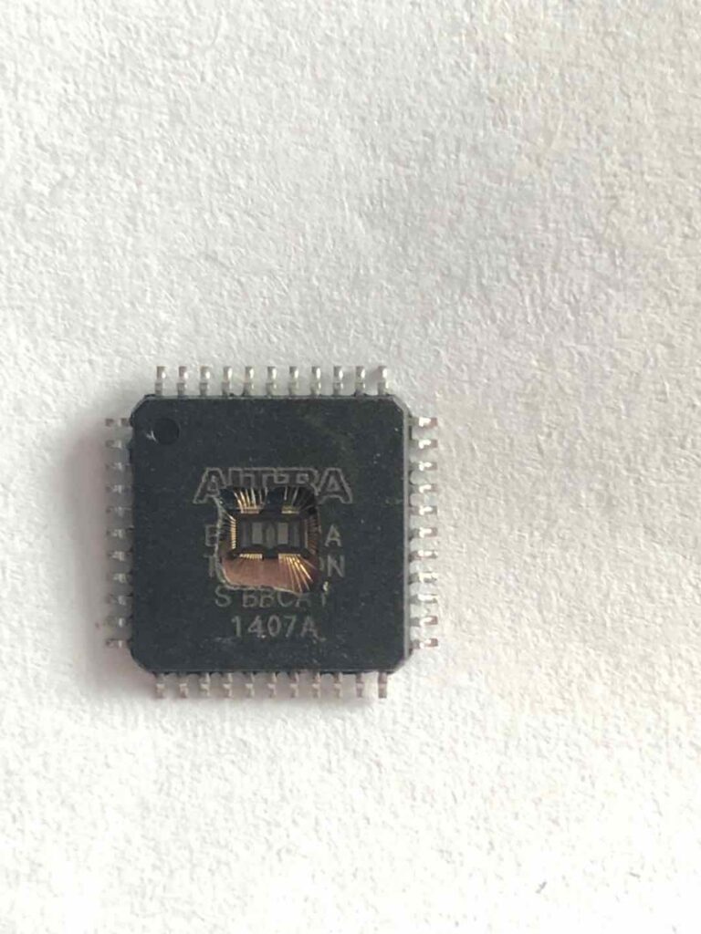
The D-line members use the e200z0h core, a 32-bit Power Architecture implementation that executes the compact Variable Length Encoding instruction set at 48 MHz. That core is single-issue and optimized for code density, which is why these parts ship with a large flash but modest RAM. Because code flash and data flash have different sector rules, an archive manifest must keep the two arrays in separate files. The 48 MHz e200z0h design is the defining feature of the D ordering line. Decapsulation can confirm a die marking on a protected microprocessor; it cannot return a locked memory array without the owner’s build archive.
Array sizes and image structure
Code storage is 128 Kbytes on the 5601 and 256 Kbytes on the 5602, with 12 or 16 Kbytes of SRAM and a 4 Kbyte data Flash block used for EEPROM emulation. The 128 / 256 KB code Flash / 12 / 16 KB SRAM / 4 KB data Flash table is the ordering reference for this line. A comparable recovery note is SPC5603BK0CLQ4R flash documentation.
Why a locked read returns nothing
| Item | What the data sheet states |
|---|---|
| Part | e200z0h at 48 MHz / 256 KB code Flash / 16 KB SRAM / LQFP64 |
| Core | e200z0h, 32-bit Power Architecture VLE, 48 MHz, single core, 3.0-5.5 V |
| Memory | 128 / 256 KB code Flash / 12 / 16 KB SRAM / 4 KB data Flash (EEPROM emulation) |
| Program memory | on-chip code Flash with ECC plus a separate data Flash block for EEPROM emulation |
| RAM | 12 KB (5601D) or 16 KB (5602D) on-chip SRAM |
| Package | LQFP64 / LQFP100, -40 to 105 or 125 C, tray or tape-and-reel |
| Boot interface | Boot Assist Module (BAM) loads code from a serial channel after reset |
Protection on these MPC56xx parts is a censorship state held in the flash configuration, not a cryptographic service. The Boot Assist Module can load a new application through a supported serial channel, but that path writes code rather than reading a protected array back out. A mass erase clears the protection and the application together, so an owner’s signed build archive is the stronger evidence. Further reading on adjacent SPC56 and MCU boards: SPC5604PGF1VLQ6 flash documentation.
Watchdog, ports and reset behaviour
The peripheral set includes one FlexCAN controller, three LINFlex serial channels, two DSPI modules, a 12-bit successive-approximation ADC and up to four periodic interrupt timers. A trailing R on the ordering code means reel packing; it does not indicate a different protection scheme. The on-chip voltage regulator allows a single supply rail, and the internal RC oscillator can avoid a crystal in cost-sensitive boards. Any reconstruction should record the clock source, theCAN bit timing and the ADC trigger setup, because all three are board specific. The terms software, program, file and firmware overlap in an enquiry, yet a cloned or duplicated image is only useful when its register map is documented. The wider NXP, ST and general MCU material is linked here: SPC5601DF1MLL4 flash documentation.
Sibling parts on the same footprint
Ordering suffixes encode the flash size, package, temperature range and packing: MLL4 marks a 100-pin LQFP, VLH4 a 64-pin LQFP and a trailing R tape-and-reel instead of tray. The 100-pin body exposes more I/O and ADC channels, so a firmware image built for it will not map cleanly onto the 64-pin part. The marked code, not the schematic, is the reliable way to tell a 5601 from a 5602 on a board whose silk screen has worn off. Related device notes on this site cover the wider Power Architecture MCU family: Arm locked cpu stm32f071rb Flash data recovery.
Service boundaries and deliverables
Within the MPC56xx range the D-line sits below the B and C lines in flash capacity but shares the e200z0h instruction set and most peripherals. Boards are often pin-compatible across capacities, which means a part can be swapped and appear to boot until the linker map overruns. The P-line parts add 64 MHz operation and, on some members, FlexRay; they are a different ordering group. Our engagement starts with a written identification record: package marking, ordering code, device identification, clock source and supply rails, followed by a comparison with the owner’s archived build. Where it is on, the deliverable is documentation rather than a promise, and the mass-erase consequence is stated in writing before any destructive step. The on-chip regulator lets a single rail run the part, which changes the decoupling check during rework. We work under NDA for the owner or an appointed repair partner and never quote a readout that depends on defeating the protection state. For background on a neighbouring automotive controller, see Arm MCU stm32f031c4 Flash memory breaking.
Owners considering duplicate SPC5602DF1VLH4R encrypted MCU software should expect a technical deliverable first: a datasheet-based identification record, a labelled image where the protection state permits one, and a clear written statement where it does not. We explain that a mass erase removes the firmware together with the protection, require written authorisation before any destructive step, and never price a service that depends on defeating the protection state. That boundary is what keeps a recovered program file usable as evidence years later.
Clone SPC5602PEF0MLH6 locked binary file
To clone SPC5602PEF0MLH6 locked binary file responsibly you first need the program array, the boot interface and the protection behaviour of the device in front of you. The SPC5602PEF0MLH6 belongs to the SPC56 / MPC56xx automotive family, and its data sheet separates what is readable from what is not. The 0MLH6 ending marks the 64-pin LQFP, 64 MHz member with 256 Kbytes of flash and 20 Kbytes of RAM.
Framing a clone SPC5602PEF0MLH6 locked binary file request
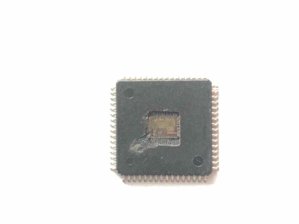
The P-line raises the e200z0h core to 64 MHz and pairs it with a larger SRAM budget than the D parts, which is why these devices appear in body, chassis and safety-related controllers. Communication is broader than the D line: FlexCAN controllers, LINFlex channels, DSPI and, on the G-suffix members, a FlexRay module for deterministic chassis networks. An eDMA controller offloads block transfers, and a fault collection and control unit gathers safety events. A duplicate or clone built from an unverified dump is less useful than a documented original, because the configuration values are board specific.
Application code versus data flash
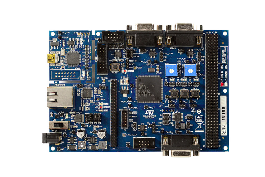
Code flash is 256 Kbytes on the 5602 and 512 Kbytes on the 5604, with 20 or 40 Kbytes of SRAM and a data flash region for EEPROM emulation. Because code and data flash have different erase geometries, an archive has to name each array; a single flat image loses that boundary. A 64-pin body has fewer ADC channels than the 144-pin part, so a captured image may reference pins that do not exist. ECC protects the code flash and the SRAM, and the error correction status module records corrected and uncorrectable events that belong in any diagnostic note. The surrounding microcontroller cross-reference is documented in SPC5602DF1VLH4R flash documentation.
Protection, ECC and mass erase
| Item | What the data sheet states |
|---|---|
| Part | e200z0h at 64 MHz / 256 KB code Flash / 20 KB SRAM / LQFP64 |
| Core | e200z0h, 32-bit Power Architecture VLE, 64 MHz, single core, 3.0-5.5 V |
| Memory | 256 / 512 KB Flash / 20 / 40 KB SRAM / 64 MHz / FlexRay on G members |
| Program memory | on-chip code Flash with ECC plus a data Flash block for EEPROM emulation |
| RAM | 20 KB (5602P) or 40 KB (5604P) on-chip SRAM |
| Package | LQFP64 / LQFP100 / LQFP144, -40 to 105 or 125 C, tray or reel |
| Boot interface | Boot Assist Module (BAM) plus a CAN/UART serial bootstrap loader |
Censorship is a configuration state held in the flash, and with it set a debug probe cannot read the flash or SRAM contents even though the device still identifies itself. The Boot Assist Module and the CAN/UART loader write code into the device; they are programming paths, not a way to read a protected image back out. For an authorised owner the deliverable is an identification record plus an archive comparison. A comparable recovery note is SPC5604BK0CLQ6 flash documentation.
The clock tree in practice
The peripheral inventory includes multiple FlexCAN channels, LINFlex UARTs, DSPI modules, a 10 or 12-bit ADC with cross triggering, eDMA and a software watchdog. G-suffix members add a FlexRay controller with dual or single channel operation and up to 10 Mbit per second, which is the feature that separates them in a chassis design. A reconstructed firmware record should capture the FlexCAN bit timing, the FlexRay configuration where present and the eDMA channel map. Decapsulation can confirm a die marking on an integrated circuit; it cannot return locked memory, and the data flash sits on the same die. Further reading on adjacent SPC56 and MCU boards: SPC56AP54L5 flash documentation.
Identifying the fitted ordering code
Ordering codes select 64, 100 or 144-pin LQFP bodies as well as temperature grade and packing. The FlexRay block on a G-suffix member changes the board harness, so its configuration belongs in a service note. The MLH6 ending marks a 64-pin body, MLL6 a 100-pin and VLQ6 a 144-pin, and the G letter in PGF1 marks the FlexRay-carrying variant. The larger body exposes more I/O and ADC channels, so a schematic is not enough to prove which package is fitted. The wider NXP, ST and general MCU material is linked here: Archive pic24fj256da210 locked firmware image.
Documentation, service and consent
The P-line shares the e200z0h core with the D, B and C lines but runs faster and carries more RAM and safety peripherals. For the ST-built SPC56 P and AP lines the silicon is the same family by origin but sold under a different brand, which is worth recording accurately. Flash size, SRAM size and the presence of FlexRay are the three facts that identify the fitted member. A written scope covers marking, ordering code, device identification, clock source, supply rails and the safety configuration, then compares the owner’s release archive with what the fitted device reports. Related device notes on this site cover the wider Power Architecture MCU family: Arm 32 bits microprocessor stm32f051c6 Flash heximal restoration.
To discuss clone SPC5602PEF0MLH6 locked binary file for a specific module, send the marking, the schematic if available and the reason the original build output is no longer accessible. We return a feasibility note that separates what the silicon exposes from what would require destroying the application, and we only proceed after the owner confirms the scope in writing. Automotive Power Architecture controllers are our regular work, and the handover is a documented file set rather than an undocumented promise about a locked chip.
Retrieve SPC5601PEF protected program data
Requests to retrieve SPC5601PEF protected program data commonly arrive after a vehicle programme stops supporting an old Power Architecture controller. The SPC5601PEF is well documented, so a careful reading of its memory map answers most of the question. PEF is the MPC560xP family prefix; a complete ordering code adds the flash size, package and temperature fields.
The retrieve SPC5601PEF protected program data question and the e200 core
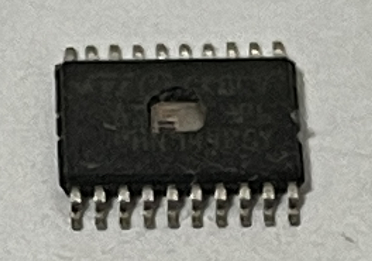
The P-line raises the e200z0h core to 64 MHz and pairs it with a larger SRAM budget than the D parts, which is why these devices appear in body, chassis and safety-related controllers. The core executes Power Architecture VLE code and remains single-issue, and a crossbar switch connects it to flash and to the peripheral bridges. The 64 MHz e200z0h core and the FlexRay option define this ordering group. The words firmware, program, file and software are often used interchangeably in an enquiry, yet they describe different artefacts on this integrated circuit.
How the memory map is divided
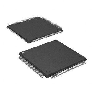
Code flash is 256 Kbytes on the 5602 and 512 Kbytes on the 5604, with 20 or 40 Kbytes of SRAM and a data flash region for EEPROM emulation. ECC protects the code flash and the SRAM, and the error correction status module records corrected and uncorrectable events that belong in any diagnostic note. The 256 / 512 KB Flash / 20 / 40 KB SRAM / 64 MHz specification is the ordering reference for the P line. For background on a neighbouring automotive controller, see SPC5602PEF0MLH6 flash documentation.
Reading a protected sample
| Item | What the data sheet states |
|---|---|
| Part | e200z0h at 64 MHz / MPC560xP family prefix / package suffix required |
| Core | e200z0h, 32-bit Power Architecture VLE, 64 MHz, single core, 3.0-5.5 V |
| Memory | 256 / 512 KB Flash / 20 / 40 KB SRAM / 64 MHz / FlexRay on G members |
| Program memory | on-chip code Flash with ECC plus a data Flash block for EEPROM emulation |
| RAM | 20 KB (5602P) or 40 KB (5604P) on-chip SRAM |
| Package | LQFP64 / LQFP100 / LQFP144, -40 to 105 or 125 C, tray or reel |
| Boot interface | Boot Assist Module (BAM) plus a CAN/UART serial bootstrap loader |
Censorship is a configuration state held in the flash, and with it set a debug probe cannot read the flash or SRAM contents even though the device still identifies itself. A mass erase clears the state and erases the application in the same operation. ECC on both flash and SRAM means an error-status log is part of a defensible diagnostic record. The FlexRay controller, the eDMA engine and the safety monitor are legitimate peripherals, not a service backdoor. The surrounding microcontroller cross-reference is documented in SPC5603CK0CLL6 flash documentation.
CAN, ADC and timer notes
The peripheral inventory includes multiple FlexCAN channels, LINFlex UARTs, DSPI modules, a 10 or 12-bit ADC with cross triggering, eDMA and a software watchdog. G-suffix members add a FlexRay controller with dual or single channel operation and up to 10 Mbit per second, which is the feature that separates them in a chassis design. Timers include a system timer module, periodic interrupt timers and a real-time counter, while the fault collection unit drives safe-state behaviour. Whether the target is source code, a heximal, a binary or configuration data, the first step on a protected chip is identical: read the identification and the reported array size. A comparable recovery note is SPC560P54L5 flash documentation.
Bodies and suffixes for the SPC5601PEF
Ordering codes select 64, 100 or 144-pin LQFP bodies as well as temperature grade and packing. The larger body exposes more I/O and ADC channels, so a schematic is not enough to prove which package is fitted. A trailing R means tape-and-reel packing and does not change the flash or the protection behaviour. Further reading on adjacent SPC56 and MCU boards: Altera cpld epm7256atc144 chip EEPROM data decoding.
What an owner can expect in writing
The P-line shares the e200z0h core with the D, B and C lines but runs faster and carries more RAM and safety peripherals. A 64-pin body has fewer ADC channels than the 144-pin part, so a captured image may reference pins that do not exist. Several members are pin-compatible, so a board can accept a smaller flash part until the application overruns it. Flash size, SRAM size and the presence of FlexRay are the three facts that identify the fitted member. A written scope covers marking, ordering code, device identification, clock source, supply rails and the safety configuration, then compares the owner’s release archive with what the fitted device reports. With censorship disabled we can return labelled code and data flash images; with it enabled we supply documentation and an archive comparison. The wider NXP, ST and general MCU material is linked here: Altera programmable logic device epm7128buc169 firmware restoration.
Any retrieve SPC5601PEF protected program data request is handled the same way on every SPC56 board: identify the fitted line, record the memory map and clock tree, then compare the customer’s archived build output with what the debug interface reports. Where the array is unprotected a labelled program file can be returned; where it is protected we supply an identification and documentation package instead. All work is scoped in writing for the owner or an authorised agent, with the erase consequence stated up front.
Decode SPC5601DF1MLL4 secured flash firmware
Anyone who has to decode SPC5601DF1MLL4 secured flash firmware usually starts with a legacy automotive board, a faded marking and no build archive. This page sets out what the SPC5601DF1MLL4 actually exposes before any tool is connected, and where the technical limits of that work sit. The MLL4 suffix fixes a 100-pin LQFP body with 128 Kbytes of flash and 12 Kbytes of SRAM on the e200z0h core.
Why decode SPC5601DF1MLL4 secured flash firmware starts with the core
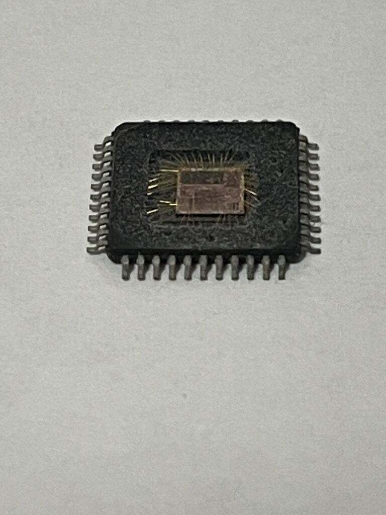
The D-line members use the e200z0h core, a 32-bit Power Architecture implementation that executes the compact Variable Length Encoding instruction set at 48 MHz. Because code flash and data flash have different sector rules, an archive manifest must keep the two arrays in separate files. A crossbar switch links the core, the flash and the peripheral bridges, and a frequency-modulated PLL derives the bus clock from a crystal or an internal RC source. Bus interfaces are the automotive basics: FlexCAN, LINFlex UARTs, DSPI and a 12-bit ADC with a programmable cross-trigger unit. That distinction matters when the deliverable is source code or a binary archive rather than a bare photograph of the decapsulated chip.
Program memory and SRAM geometry
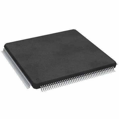
Code storage is 128 Kbytes on the 5601 and 256 Kbytes on the 5602, with 12 or 16 Kbytes of SRAM and a 4 Kbyte data Flash block used for EEPROM emulation. The 128 / 256 KB code Flash / 12 / 16 KB SRAM / 4 KB data Flash table is the ordering reference for this line. Related device notes on this site cover the wider Power Architecture MCU family: SPC5601PEF flash documentation.
Censorship and what the interface can report
| Item | What the data sheet states |
|---|---|
| Part | e200z0h at 48 MHz / 128 KB code Flash / 12 KB SRAM / LQFP100 |
| Core | e200z0h, 32-bit Power Architecture VLE, 48 MHz, single core, 3.0-5.5 V |
| Memory | 128 / 256 KB code Flash / 12 / 16 KB SRAM / 4 KB data Flash (EEPROM emulation) |
| Program memory | on-chip code Flash with ECC plus a separate data Flash block for EEPROM emulation |
| RAM | 12 KB (5601D) or 16 KB (5602D) on-chip SRAM |
| Package | LQFP64 / LQFP100, -40 to 105 or 125 C, tray or tape-and-reel |
| Boot interface | Boot Assist Module (BAM) loads code from a serial channel after reset |
Protection on these MPC56xx parts is a censorship state held in the flash configuration, not a cryptographic service. When censorship is active, debug access to the flash and SRAM contents is blocked while the device still returns its identification. The ADC, the CAN controller and the PLL are application features and provide no alternate readout route. For background on a neighbouring automotive controller, see SPC5603BK0CLQ4R flash documentation.
Peripheral inventory worth recording
The peripheral set includes one FlexCAN controller, three LINFlex serial channels, two DSPI modules, a 12-bit successive-approximation ADC and up to four periodic interrupt timers. The on-chip voltage regulator allows a single supply rail, and the internal RC oscillator can avoid a crystal in cost-sensitive boards. A trailing R on the ordering code means reel packing; it does not indicate a different protection scheme. Any reconstruction should record the clock source, theCAN bit timing and the ADC trigger setup, because all three are board specific. The surrounding microcontroller cross-reference is documented in SPC5604PGF1VLQ6 flash documentation.
Ordering codes, bodies and rails
Ordering suffixes encode the flash size, package, temperature range and packing: MLL4 marks a 100-pin LQFP, VLH4 a 64-pin LQFP and a trailing R tape-and-reel instead of tray. The 100-pin body exposes more I/O and ADC channels, so a firmware image built for it will not map cleanly onto the 64-pin part. The marked code, not the schematic, is the reliable way to tell a 5601 from a 5602 on a board whose silk screen has worn off. A comparable recovery note is Altera cpld epm7064aetc100 chip protection breaking.
Scope of an authorised engagement
Within the MPC56xx range the D-line sits below the B and C lines in flash capacity but shares the e200z0h instruction set and most peripherals. Boards are often pin-compatible across capacities, which means a part can be swapped and appear to boot until the linker map overruns. The P-line parts add 64 MHz operation and, on some members, FlexRay; they are a different ordering group. Our engagement starts with a written identification record: package marking, ordering code, device identification, clock source and supply rails, followed by a comparison with the owner’s archived build. The on-chip regulator lets a single rail run the part, which changes the decoupling check during rework. Where it is on, the deliverable is documentation rather than a promise, and the mass-erase consequence is stated in writing before any destructive step. We work under NDA for the owner or an appointed repair partner and never quote a readout that depends on defeating the protection state. Further reading on adjacent SPC56 and MCU boards: Altera cpld epm7128alc embedded EEPROM program recovery.
If you need to decode SPC5601DF1MLL4 secured flash firmware, the practical first step is a written identification report: package marking, ordering code, device identification, clock source and supply rails, followed by a comparison with any build archive you hold. Our engineers document those findings, explain whether a clean read is possible, and state the mass-erase limit before any destructive work is authorised. We work under NDA for legitimate owners and their appointed repair partners, and we do not quote a readout that depends on suppressing a protection state.