

The IC C8051F530 is a powerful 8-bit microcontroller from Silicon Labs, featuring an enhanced 8051 core, integrated analog and digital peripherals, and on-chip Flash memory and EEPROM. Commonly used in industrial control systems, commercial electronics, and IoT devices, the C8051F530 is designed for embedded applications that demand reliability, low power consumption, and compact design.
O processo para atacar e clonar o firmware do C8051F530 envolve várias etapas técnicas: Identificação do Dispositivo e Configuração da Interface Começamos analisando o encapsulamento e os protocolos de comunicação do microcontrolador. O C8051F530 suporta programação no sistema por meio de sua interface C2, que acessamos usando ferramentas de hardware personalizadas. Mapeamento de Memória e Bypass de Proteção Nosso próximo passo é avaliar as configurações de proteção da memória. Muitos sistemas protegidos habilitam a proteção contra leitura de código (CRP) para impedir a extração do firmware. Aplicamos métodos não invasivos e semi-invasivos para ignorar essas proteções, dependendo da configuração do sistema. Despejando Flash e EEPROM Uma vez obtido o acesso, procedemos à cópia ou duplicação do conteúdo da memória Flash, EEPROM e outros blocos de memória. Os dados binários ou hexagonais são então armazenados em arquivos para processamento posterior.
However, the firmware stored in the Flash memory of this IC is often locked, encrypted, or otherwise protected to prevent reverse engineering or unauthorized access. This can pose challenges for engineers, security researchers, and developers who need to restore, crack, or decode the firmware for legitimate reasons—such as recovery, debugging, or system integration. At CIRCUIT ENGINEERING CO.,LTD, we specialize in services to attack IC C8051F530 firmware, helping clients unlock and extract secured system data with precision and confidentiality.
Understanding the Attack Process
The process to attack and clone the C8051F530 firmware involves several technical steps:
-
Device Identification & Interface Setup
We begin by analyzing the microcontroller’s packaging and communication protocols. The C8051F530 supports in-system programming via its C2 interface, which we tap into using custom hardware tools. -
Memory Mapping & Protection Bypass
Our next step is to assess memory protection settings. Many protected systems enable code read protection (CRP) to prevent firmware extraction. We apply non-invasive and semi-invasive methods to bypass these protections, depending on the system configuration. -
Dumping Flash & EEPROM
Once access is gained, we proceed to copy or duplicate the contents of Flash memory, EEPROM, and other memory blocks. The binary or heximal data is then dumped into files for further processing. -
Decryption & Decompilation
If the firmware is encrypted, we use advanced techniques to decrypt the data. The resulting binary is then reverse-engineered to decode the logic and convert it into C/C++ source code or assembly, depending on client needs. -
Analysis & Reconstruction
The final step involves reconstructing the program logic, analyzing the extracted firmware archive, and optionally cloning it to a new chip for duplication or emulation purposes.
Процесс атаки и клонирования прошивки C8051F530 включает несколько технических шагов: Идентификация устройства и настройка интерфейса Мы начинаем с анализа упаковки и протоколов связи микроконтроллера. C8051F530 поддерживает внутрисистемное программирование через свой интерфейс C2, к которому мы подключаемся с помощью специальных аппаратных инструментов. Отображение памяти и обход защиты Наш следующий шаг — оценка настроек защиты памяти. Многие защищенные системы включают защиту от чтения кода (CRP) для предотвращения извлечения прошивки. Мы применяем неинвазивные и полуинвазивные методы для обхода этих защит в зависимости от конфигурации системы. Сброс Flash и EEPROM После получения доступа мы приступаем к копированию или дублированию содержимого Flash-памяти, EEPROM и других блоков памяти. Двоичные или шестнадцатеричные данные затем сбрасываются в файлы для дальнейшей обработки.
Why Clients Choose Us
-
Proven Track Record: Years of experience in firmware cracking, binary analysis, and hardware reverse engineering.
-
Tailored Services: We support a wide range of secured devices, including locked, embedded systems across multiple industries.
-
Confidentiality & Compliance: All projects are handled securely with full client confidentiality and compliance with applicable laws.
Whether you need to hack, clone, or open the source code of a C8051F530 system, our expert team is equipped to deliver efficient and ethical solutions. Contact us today to discuss how we can help you unlock your protected firmware and recover valuable program files and data archives.

Attack IC C8051F530 protective system and remove its security fuse bit, extract firmware out from MCU C8051F530 flash memory, copy heximal to blank Microcontroller C8051F530 which will provide the same functions
Attack IC C8051F530 protective system and remove its security fuse bit, extract firmware out from MCU C8051F530 flash memory, copy heximal to blank Microcontroller C8051F530 which will provide the same functions;
Analog Peripherals
– 12-Bit ADC
· ±1 LSB INL (C8051F52x/C8051F53x); no missing codes
· Programmable throughput up to 200 ksps
· Up to 6/16 external inputs
· Data dependent windowed interrupt generator
· Built-in temperature sensor
– Comparator
· Programmable hysteresis and response time
· Configurable as wake-up or reset source
· Low current
– POR/Brownout Detector
– Voltage Reference—1.5 to 2.2 V (programmable)
On-Chip Debug
– On-chip debug circuitry facilitates full-speed, non-intrusive in-system debug (No emulator required)
– Provides breakpoints, single stepping
– Inspect/modify memory and registers
– Complete development kit
Supply Voltage 2.7 to 5.25 V
– Built-in LDO regulator
High Speed 8051 µC Core
– Pipelined instruction architecture; executes 70% of instructions in 1 or 2 system clocks
– Up to 25 MIPS throughput with 25 MHz system clock
Il processo di attacco e clonazione del firmware C8051F530 prevede diverse fasi tecniche:Iniziamo analizzando il packaging e i protocolli di comunicazione del microcontrollore. Il C8051F530 supporta la programmazione in-system tramite la sua interfaccia C2, che utilizziamo utilizzando strumenti hardware personalizzati.Il nostro passo successivo consiste nel valutare le impostazioni di protezione della memoria. Molti sistemi protetti abilitano la protezione dalla lettura del codice (CRP) per impedire l’estrazione del firmware. Applichiamo metodi non invasivi e semi-invasivi per bypassare queste protezioni, a seconda della configurazione del sistema.Una volta ottenuto l’accesso, procediamo a copiare o duplicare il contenuto della memoria Flash, della EEPROM e di altri blocchi di memoria. I dati binari o esadecimali vengono quindi scaricati in file per un’ulteriore elaborazione.
Memory
– 8/4/2 kB Flash; In-system byte programmable in 512 byte sectors
– 256 bytes internal data RAM
Digital Peripherals
– 16/6 port I/O; push-pull or open-drain, 5 V tolerant
– Hardware SPI™, and UART serial port
– Hardware LIN (both master and slave, compatible with V1.3 and V2.0)
– Three general purpose 16-bit counter/timers
– Programmable 16-bit counter/timer array with three capture/compare modules, WDT
Clock Sources
– Internal oscillators: 24.5 MHz ±0.5% accuracy supports UART and LIN-Master operation
– External oscillator: Crystal, RC, C, or Clock (1 or 2 pin modes)
– Can switch between clock sources on-the-fly
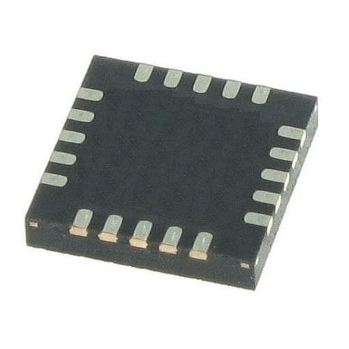
Packages:
– 10-Pin QFN (3 x 3 mm)
– 20-pin QFN (4 x 4 mm)
– 20-pin TSSOP
Temperature Range: –40 to +125 °C