Posts Tagged ‘schematic diagram’
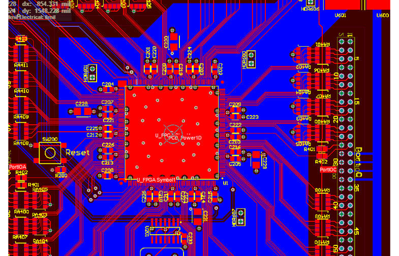
 PCB Schematic Diagram Design proces
The design of schematic diagram should use SCHEMATIC DIAGRAM design system of PROTEL98 or PROTEL99SE to draw a schematic diagram, it is the foundation of circuit board design project. During this process, designer should take advantage of all kinds of drawing tools and edit functions provided by software, the process is see below:
1. Start-up: open up PROTEL98 schematic diagram editor:
Click “Start” bottom, and choose PROTEL98 inthe “Program”.
2. Install circuit drawing dimension and layout
User can install the dimension, orientation and grid size of drawing and title.
3. Place necessary components on the schematic diagram
User select the necessary components from database and place them onto the right place according to circuit schematic diagram requirement, as well as modification.
4. Layout the components which have been placed
Use line and signal to connect all the components on platform to constitute a complete schematic diagram
5. Modify components after PCB layout
In order to ensure the schematic diagram’s preciseness and aesthetic, components location need to be modify through delete, move and adjust drawing size, feature and orientation.
6. Save file and print output
Save schematic diagram which has been edited and print it out for file.
PCB Circuit Board Schematic Diagram Drawing Process
PCB Circuit Board Schematic Diagram Drawing Process include add the new files, and install working environment, placing electronic components, then layout the schematic diagram:
1 Add new SCH file:
Before entering SCH design system, first you should have general image of the schematic diagram you are about to draw, that is to say you have to understand what circuit need to use on the design of your schematic diagram, and then use PROTEL DXP to draw schematic diagram;
2 Install working environment:
You should choose the right size of drawing paper according to the complexity level of circuit pattern. During the whole process of circuit design, size of drawing paper can be adjusted so set up the proper size of drawing paper could be defined as the 1st step of schematic diagram drawing.
3 Component placement:
Choose components from library, dissipate them onto proper location of drawing and define their name, package method, Adjust and modify the locations of each components according to their electronic connection and circuit relations to make it more reliable and easy to understand.
4 Layout of Schematic Diagram:
Layout schematic diagram according to the requirement of circuit pattern by using different kinds of tools and instruction provide by SCH software, connect all the components on the surface through their electrical connection by circuit and symbol, to form a complete schematic diagram.