Posts Tagged ‘reverse engineering chip program’
 Reverse Engineering Chip PIC12C508 Code
Reverse Engineering Chip PIC12C508 Code need to extract the embedded firmware from locked microcontroller pic12c508, then crack mcu protective system;
The recommendations of the maximum receiver baud rate error was made under the assumption that the Receiver and Transmitter equally divides the maximum total error. There are two possible sources for the receivers baud rate error. The Receiver’s system clock (XTAL) will always have some minor instability over the supply voltage range and the temperature range.
When using a crystal to generate the system clock, this is rarely a problem, but for a resonator the system clock may differ more than 2% depending of the resonators tolerance. The second source for the error is more controllable. The baud rate generator can not always do an exact division of the system frequency to get the baud rate wanted after copy mcu pic16f870 program.
In this case an UBRR value that gives an acceptable low error can be used if possible. Setting the Multi-processor Communication mode (MPCMn) bit in UCSRnA enables a filtering function of incoming frames received by the USART Receiver.
Frames that do not contain address information will be ignored and not put into the receive buffer. This effectively reduces the number of incoming frames that has to be handled by the CPU, in a system with multiple CHIPs that communicate via the same serial bus if attacking mcu c8051f530 firmware.
The Transmitter is unaffected by the MPCMn setting, but has to be used differently when it is a part of a system utilizing the Multi-processor Communication mode. If the Receiver is set up to receive frames that contain 5 to 8 data bits, then the first stop bit indicates if the frame contains data or address information. If the Receiver is set up for frames with nine data bits, then the ninth bit (RXB8n) is used for identifying address and data frames.
When the frame type bit (the first stop or the ninth bit) is one, the frame contains an address. When the frame type bit is zero the frame is a data frame.
The Multi-processor Communication mode enables several slave CHIPs to receive data from a master CHIP. This is done by first decoding an address frame to find out which CHIP has been addressed if attack microcontroller pic16c63a hex.
If a particular slave CHIP has been addressed, it will receive the following data frames as normal, while the other slave CHIPs will ignore the received frames until another address frame is received.
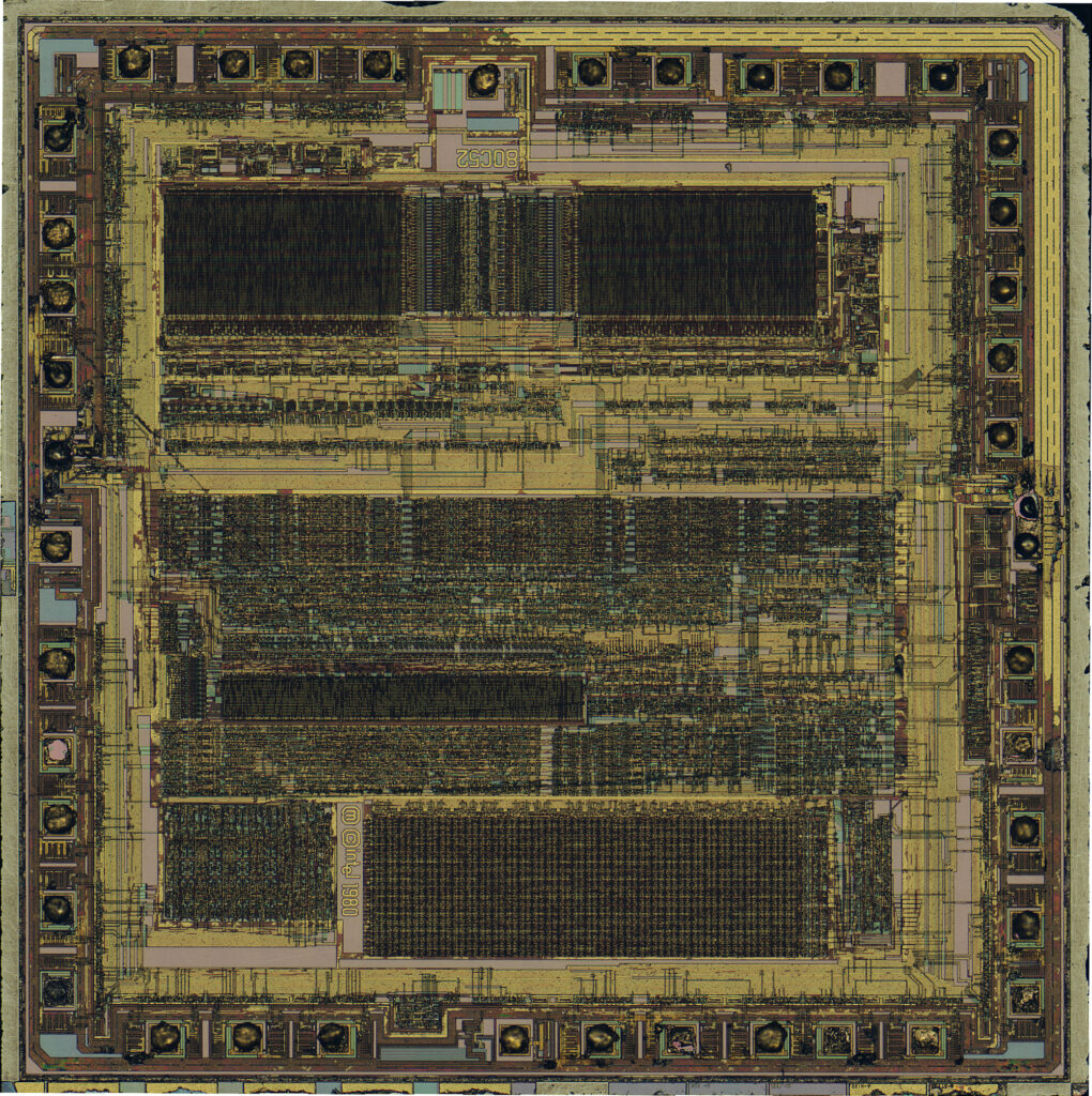
Reverse Engineering Chip ATmega2560L Software
Reverse Engineering Chip ATmega2560L Software is actually a process to read encrypted heximal from mcu atmega2560L flash memory after crack microcontroller atmega2560L security fuse bit;
The Timer/Counter can be clocked by an internal synchronous or an external asynchronous clock source. The clock source clkT2 is by default equal to the MCU clock, clkI/O.
When the AS2 bit in the ASSR Register is written to logic one, the clock source is taken from the Timer/Counter Oscillator connected to TOSC1 and TOSC2. For details on asynchronous operation, see “Asynchronous Status Register – ASSR” on page 189 if attack attiny2313 mcu firmware.
For details on clock sources and prescaler, see “Timer/Counter Prescaler” on page 193. The main part of the 8-bit Timer/Counter is the programmable bi-directional counter unit.
Figure 68 shows a block diagram of the counter and its surrounding environment. Depending on the mode of operation used, the counter is cleared, incremented, or decremented at each timer clock (clkT2). clkT2 can be generated from an external or internal clock source, selected by the Clock Select bits (CS22:0) before attack atmega64l mcu flash.
When no clock source is selected (CS22:0 = 0) the timer is stopped. However, the TCNT2 value can be accessed by the CPU, regardless of whether clkT2 is present or not. A CPU write overrides (has priority over) all counter clear or count operations.
The counting sequence is determined by the setting of the WGM21 and WGM20 bits located in the Timer/Counter Control Register (TCCR2A) and the WGM22 located in the Timer/Counter Control Register B (TCCR2B).
There are close connections between how the counter behaves (counts) and how waveforms are generated on the Output Compare outputs OC2A and OC2B. For more details about advanced counting sequences and waveform generation, see “Modes of Operation” on page 178.
The Timer/Counter Overflow Flag (TOV2) is set according to the mode of operation selected by the WGM22:0 bits. TOV2 can be used for generating a CPU interrupt.
The 8-bit comparator continuously compares TCNT2 with the Output Compare Register (OCR2A and OCR2B). Whenever TCNT2 equals OCR2A or OCR2B, the comparator signals a match. A match will set the Output Compare Flag (OCF2A or OCF2B) at the next timer clock cycle.
If the corresponding interrupt is enabled, the Output Compare Flag generates an Output Compare interrupt. The Output Compare Flag is automatically cleared when the interrupt is executed.
Alternatively, the Output Compare Flag can be cleared by software by writing a logical one to its I/O bit location. The Waveform Generator uses the match signal to generate an output according to operating mode set by the WGM22:0 bits and Compare Output mode (COM2x1:0) bits.
The max and bottom signals are used by the Waveform Generator for handling the special cases of the extreme values in some modes of operation (“Modes of Operation” on page 178). Figure 58 on page 154 shows a block diagram of the Output Compare unit.