Posts Tagged ‘recover microcontroller source file’
 Recover Microcontroller STM32F105RCT6TR Binary
Recover Microcontroller STM32F105RCT6TR Binary
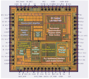
We can Recover Microcontroller STM32F105RCT6TR Binary, please view below Microcontroller STM32F105RCT6TR features for your reference:
Features
Core: ARM 32-bit Cortex™-M3 CPU
– 72 MHz maximum frequency, 1.25 DMIPS/MHz (Dhrystone 2.1) performance at 0 wait state memory
LQFP100 14 × 14 mm
LQFP64 10 × 10 mm
access
– Single-cycle multiplication and hardware division
Memories
– 64 to 256 Kbytes of Flash memory
– up to 64 Kbytes of general-purpose SRAM Clock, reset and supply management
– 2.0 to 3.6 V application supply and I/Os
– POR, PDR, and programmable voltage detector (PVD)
– 3-to-25 MHz crystal oscillator
– Internal 8 MHz factory-trimmed RC
– Internal 40 kHz RC with calibration
– 32 kHz oscillator for RTC with calibration Low power
– Sleep, Stop and Standby modes
– VBAT supply for RTC and backup registers
2 × 12-bit, 1 µs A/D converters (16 channels)
– Conversion range: 0 to 3.6 V
– Sample and hold capability
– Temperature sensor
– up to 2 MSPS in interleaved mode 2 × 12-bit D/A converters DMA: 12-channel DMA controller
– Supported peripherals: timers, ADCs, DAC, I2Ss, SPIs, I2Cs and USARTs
Up to 10 timers with pinout remap capability
– Up to four 16-bit timers, each with up to 4 IC/OC/PWM or pulse counter and quadrature (incremental) encoder input
– 1 × 16-bit motor control PWM timer with dead-time generation and emergency stop
– 2 × watchdog timers (Independent and Window)
– SysTick timer: a 24-bit downcounter
– 2 × 16-bit basic timers to drive the DAC Up to 14 communication interfaces with pinout remap capability
– Up to 2 × I2C interfaces (SMBus/PMBus)
– Up to 5 USARTs (ISO 7816 interface, LIN, IrDA capability, modem control)
– Up to 3 SPIs (18 Mbit/s), 2 with a multiplexed I2S interface that offers audio class accuracy via advanced PLL schemes
– 2 × CAN interfaces (2.0B Active) with 512 bytes of dedicated SRAM
– USB 2.0 full-speed device/host/OTG controller with on-chip PHY that supports HNP/SRP/ID with 1.25 Kbytes of dedicated SRAM
– 10/100 Ethernet MAC with dedicated DMA and SRAM (4 Kbytes): IEEE1588 hardware support, MII/RMII available on all packages
Table 1.
Device summary
– Serial wire debug (SWD) & JTAG interfaces
Reference
Part number
– Cortex-M3 Embedded Trace Macrocell™
Up to 80 fast I/O ports
– 51/80 I/Os, all mappable on 16 external interrupt vectors and almost all 5 V-tolerant CRC calculation unit, 96-bit unique ID
STM32F105xx
STM32F107xx
STM32F105R8, STM32F105V8
STM32F105RB, STM32F105VB
STM32F105RC, STM32F105VC
STM32F107RB, STM32F107VB
STM32F107RC, STM32F107VC
Recover Microcontroller 430G2452 Heximal
Recover Microcontroller 430G2452 Heximal out from MCU MSP430G2452 is a process start from Crack MCU MSP430G2452 protective system and disable its security fuse bit by focus ion beam, then copy the code fro new microcontroller
Recover Microcontroller 430G2452 Heximal out from MCU MSP430G2452 is a process start from Crack MCU MSP430G2452 protective system and disable its security fuse bit by focus ion beam, then copy the code fro new microcontroller;
FEATURES
Low Supply Voltage Range: 1.8 V to 3.6 V Ultra-Low Power Consumption
– Active Mode: 220 µA at 1 MHz, 2.2 V
– Standby Mode: 0.5 µA
– Off Mode (RAM Retention): 0.1 µA
Five Power-Saving Modes Ultra-Fast Wake-Up From Standby Mode in Less Than 1 µs 16-Bit RISC Architecture, 62.5-ns Instruction Cycle Time.
Basic Clock Module Configurations
– Internal Frequencies up to 16 MHz With
Four Calibrated Frequencies
– Internal Very-Low-Power Low-Frequency (LF) Oscillator
– 32-kHz Crystal
– External Digital Clock Source
One 16-Bit Timer_A With Three Capture/Compare Registers Up to 16 Touch-Sense Enabled I/O Pins
Universal Serial Interface (USI) Supporting SPI and I2C 10-Bit 200-ksps Analog-to-Digital (A/D)
Converter With Internal Reference, Sample-and-Hold, and Autoscan (MSP430G2x52 Only) On-Chip Comparator for Analog Brownout Detector Serial Onboard Programming, No External Programming Voltage Needed, Programmable Code Protection by Security Fuse On-Chip Emulation Logic With Spy-Bi-Wire Interface Family Members are Summarized:
Package Options
– TSSOP: 14 Pin, 20 Pin
– PDIP: 20 Pin
– QFN: 16 Pin
For Complete Module Descriptions, See the MSP430x2xx Family User’s Guide (SLAU144)
DESCRIPTION
The Texas Instruments MSP430™ family of ultra-low-power microcontrollers consist of several devices featuring different sets of peripherals targeted for various applications. The architecture, combined with five low-power modes, is optimized to achieve extended battery life in portable measurement applications.
The device features a powerful 16-bit RISC CPU, 16-bit registers, and constant generators that contribute to maximum code efficiency. The digitally controlled oscillator (DCO) allows wake-up from low-power modes to active mode in less than 1 µs.
The MSP430G2x52 and MSP430G2x12 series of microcontrollers are ultra-low-power mixed signal microcontrollers with built-in 16-bit timers, and up to 16 I/O touch sense enabled pins and built-in communication capability using the universal serial communication interface and have a versatile analog comparator.
The MSP430G2x52 series have a 10-bit A/D converter. For configuration details see Table 1. Typical applications include low-cost sensor systems that capture analog signals, convert them to digital values, and then process the data for display or for transmission to a host system when attacking Microcontrolle ST62T15C6 firmware memory.
Recover Microcontroller MC68HC908JB16 Firmware
Recover Microcontroller MC68HC908JB16 Firmware from flash memory include the program and data, the heximal file can be copied to new MCU MC68HC908JB16;
Recover Microcontroller MC68HC908JB16 Firmware from flash memory include the program and data, the heximal file can be copied to new MCU MC68HC908JB16
Features of the Microcontroller MC68HC908JB16 include the following:
High-performance M68HC08 architecture
Fully upward-compatible object code with M6805, M146805, and
M68HC05 families
Low-power design; fully static with stop and wait modes
6-MHz internal bus frequency
16,384 bytes of on-chip FLASH memory with security1 feature
384 bytes of on-chip random access memory (RAM)
Up to 21 general-purpose input/output (I/O) pins, including:
– 15 shared-function I/O pins
– 8-bit keyboard interrupt port
– 10mA high current drive for PS/2 connection on 2 pins (with USB module disabled)
– 1 dedicated I/O pin, with 25mA direct drive for infrared LED (32-pin package) if recover Microcontroller STM32F107RCT6 code
– 6 dedicated I/O pins, with 25mA direct drive for infrared LED on 2 pins and 10mA direct drive for normal LED on 4 pins (28-pin package)
Two 16-bit, 2-channel timer interface modules (TIM1 and TIM2) with selectable input capture, output compare, PWM capability on each channel, and external clock input option (TCLK)
Universal Serial Bus specification 2.0 low-speed functions:
– 1.5Mbps data rate
– On-chip 3.3V regulator
– Endpoint 0 with 8-byte transmit buffer and 8-byte receive buffer
– Endpoint 1 with 8-byte transmit buffer
– Endpoint 2 with 8-byte transmit buffer and 8-byte receive buffer
Serial communications interface module (SCI)
Dual clock generator modules (CGM) (32-pin package)
In-circuit programming capability using USB communication or standard serial link on PTA0 pin
System protection features:
– Optional computer operating properly (COP) reset
– Optional Low-voltage detection with reset
– Illegal opcode detection with reset
– Illegal address detection with reset
Master reset pin with internal pull-up and power-on reset
IRQ interrupt pin with internal pull-up and schmitt-trigger input
32-pin low-profile quad flat pack (LQFP) and 28-pin small outline
integrated circuit package (SOIC)
Features of the CPU08 include the following:
Enhanced HC05 programming model
Extensive loop control functions
16 addressing modes (eight more than the HC05)
16-bit index register and stack pointer
Memory-to-memory data transfers
Fast 8 × 8 multiply instruction
Fast 16/8 divide instruction
Binary-coded decimal (BCD) instructions
Optimization for controller applications
Third party C language support