Posts Tagged ‘ic breaking embedded binary’
 Break IC PIC18F242 Software
Break IC PIC18F242 Software is a process to unlock encrypted mcu pic18f242 protection and open locked microcontroller pic18f242 flash memory silicon package;
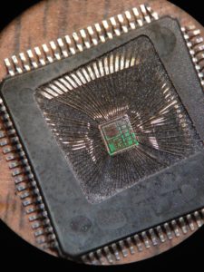
Break IC PIC18F242 Software is a process to unlock encrypted mcu pic18f242 protection and open locked microcontroller pic18f242 flash memory silicon package
High Performance RISC CPU:
· C compiler optimized architecture/instruction set
– Source code compatible with the PIC16 and PIC17 instruction sets
· Linear program memory addressing to 32 Kbytes
· Linear data memory addressing to 1.5 Kbytes
· Up to 10 MIPs operation:
– DC – 40 MHz osc./clock input
– 4 MHz – 10 MHz osc./clock input with PLL active
· 16-bit wide instructions, 8-bit wide data path
· Priority levels for interrupts
· 8 x 8 Single Cycle Hardware Multiplier
Peripheral Features:
· High current sink/source 25 mA/25 mA
· Three external interrupt pins
· Timer0 module: 8-bit/16-bit timer/counter with 8-bit programmable prescaler
· Timer1 module: 16-bit timer/counter
· Timer2 module: 8-bit timer/counter with 8-bit period register (time-base for PWM)
· Timer3 module: 16-bit timer/counter
· Secondary oscillator clock option – Timer1/Timer3
· Two Capture/Compare/PWM (CCP) modules. CCP pins that can be configured as:
– Capture input: capture is 16-bit, max. resolution 6.25 ns (TCY/16)
– Compare is 16-bit, max. resolution 100 ns (TCY)
– PWM output: PWM resolution is 1- to 10-bit, max. PWM freq. @: 8-bit resolution = 156 kHz 10-bit resolution = 39 kHz
· Master Synchronous Serial Port (MSSP) module,
Two modes of operation:
– 3-wire SPI™ (supports all 4 SPI modes)
– I2C™ Master and Slave mode
Peripheral Features (Continued):
· Addressable USART module:
– Supports RS-485 and RS-232
· Parallel Slave Port (PSP) module
Analog Features:
· Compatible 10-bit Analog-to-Digital Converter module (A/D):
– Fast sampling rate
– Conversion available during SLEEP
– Linearity ≤ 1 LSb
· Programmable Low Voltage Detection (PLVD)
– Supports interrupt on-Low Voltage Detection
· Programmable Brown-out Reset (BOR)
Break IC PIC12HV615 Heximal
Break IC PIC12HV615 Heximal
We can Break IC PIC12HV615 Heximal, please view the IC PIC12HV615 features for your reference:
To read a program memory location, the user must write two bytes of the address to the PMADRL and PMADRH registers, and then set control bit RD (PMCON1<0>). Once the read control bit is set, the program memory Flash controller will use the second instruction cycle after to read the data.
This causes the second instruction immediately following the “BSF PMCON1,RD” instruction to be ignored. The data is available in the very next cycle in the PMDATL and PMDATH registers; it can be read as two bytes in the following instructions.
PMDATL and PMDATH registers will hold this value until another read or until it is written to by the user (during a write operation). A word of the Flash program memory may only be written to if the word is in an unprotected segment of memory after Break IC.
Flash program memory must be written in four-word blocks. See Figure 3-2 and Figure 3-3 for more details. A block consists of four words with sequential addresses, with a lower boundary defined by an address, where PMADRL<1:0> = 00. All block writes to program memory are done as 16-word erase by four-word write operations. The write operation is edge aligned and cannot occur across boundaries. To write program data, it must first be loaded into the buffer registers (see Figure 3-2). This is accomplished by first writing the destination address to PMADRL and PMADRH and then writing the data to PMDATL and PMDATH.
After the address and data have been set up, then the following sequence of events must be executed:
Write 55h, then AAh, to PMCON2 (Flash programming sequence). Set the WR control bit of the PMCON1 register. All four buffer register locations should be written to with correct data. If less than four words are being written to in the block of four words, then a read from the program memory location(s) not being written to must be performed if Break IC.
This takes the data from the program location(s) not being written and loads it into the PMDATL and PMDATH registers. Then the sequence of events to transfer data to the buffer registers must be executed. To transfer data from the buffer registers to the program memory, the PMADRL and PMADRH must point to the last location in the four-word block (PMADRL<1:0> = 11). Then the following sequence of events must be executed:
Write 55h, then AAh, to PMCON2 (Flash programming sequence). Set control bit WR of the PMCON1 register to begin the write operation. The user must follow the same specific sequence to initiate the write for each word in the program block, writing each program word in sequence (000, 001, 010, 011). When the write is performed on the last word (PMADRL<1:0> = 11), a block of sixteen words is automatically erased and the content of the four-word buffer registers are written into the program memory. After the “BSF PMCON1,WR” instruction, the processor requires two cycles to set up the erase/write operation. The user must place two NOP instructions after the WR bit is set. Since data is being written to buffer registers, the writing of the first three words of the block appears to occur immediately before Break IC.
Break IC PIC16F627 Code
Break IC PIC16F627 and extract flash code from mcu pic16f627, the fuse bit of microcontroller pic16f627 will be cracked by focus ion beam;
We can Break IC PIC16F627 Code, please view the IC PIC16F627 features for your reference:
High Performance RISC CPU:
· Only 35 instructions to learn
· All single-cycle instructions (200 ns), except for program branches which are two-cycle
· Operating speed:
– DC – 20 MHz clock input
– DC – 200 ns instruction cycle Interrupt capability
16 special function hardware registers
8-level deep hardware stack
Direct, Indirect and Relative addressing modes
Peripheral Features:
· 15 I/O pins with individual direction control
· High current sink/source for direct LED drive
· Analog comparator module with:
– Two analog comparators
– Programmable on-chip voltage reference (VREF) module
– Programmable input multiplexing from device inputs and internal voltage reference
– Comparator outputs are externally accessible
· Timer0: 8-bit timer/counter with 8-bit programmable prescaler
· Timer1: 16-bit timer/counter with external crystal/ clock capability
· Timer2: 8-bit timer/counter with 8-bit period register, prescaler and postscaler
· Capture, Compare, PWM (CCP) module
– Capture is 16-bit, max. resolution is 12.5 ns
– Compare is 16-bit, max. resolution is 200 ns
– PWM max. resolution is 10-bit
· Universal Synchronous/Asynchronous Receiver/Transmitter USART/SCI
· 16 Bytes of common RAM
Special Microcontroller Features:
· Power-on Reset (POR)
· Power-up Timer (PWRT) and Oscillator Start-up Timer (OST)
· Brown-out Detect (BOD)
· Watchdog Timer (WDT) with its own on-chip RC oscillator for reliable operation
· Multiplexed MCLR-pin
· Programmable weak pull-ups on PORTB
· Programmable code protection
· Low voltage programming
· Power saving SLEEP mode
· Selectable oscillator options
– FLASH configuration bits for oscillator options
– ER (External Resistor) oscillator
– Reduced part count
– Dual speed INTRC
– Lower current consumption
– EC External Clock input
– XT oscillator mode
– HS oscillator mode
– LP oscillator mode
· Serial in-circuit programming (via two pins)
· Four user programmable ID locations
CMOS Technology:
· Low-power, high-speed CMOS FLASH technology
· Fully static design
· Wide operating voltage range
– PIC16F627 – 3.0V to 5.5V
– PIC16F628 – 3.0V to 5.5V
– PIC16LF627 – 2.0V to 5.5V
– PIC16LF628 – 2.0V to 5.5V
· Commercial, industrial and extended temperature range
· Low power consumption
– < 2.0 mA @ 5.0V, 4.0 MHz
– 15 µA typical @ 3.0V, 32 kHz
– < 1.0 µA typical standby current @ 3.0V