Posts Tagged ‘decap ic security bits’
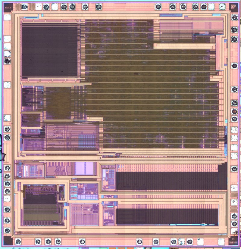
 Crack IC PIC12LC509 Security bits
Crack IC PIC12LC509 Security bits and decrypt microchip mcu pic12lc509 flash memory content out from it, extract secured code from pic12lc509 flash and eeprom memory in the format of heximal.
The MPLAB PM3 Device Programmer is a universal, CE compliant device programmer with programmable voltage verification at VDDMIN and VDDMAX for maximum reliability.
It features a large LCD display (128 x 64) for menus and error messages and a modular, detachable socket assembly to support various package types if recover mcu pic18f452 program.
The ICSP™ cable assembly is included as a standard item. In Stand-Alone mode, the MPLAB PM3 Device Programmer can read, verify and program PIC devices without a PC connection.
It can also set security bits protection in this mode. The MPLAB PM3 connects to the host PC via an RS-232 or USB cable.
The MPLAB PM3 has high-speed communications and optimized algorithms for quick programming of large memory devices and incorporates an SD/MMC card for file storage and secure data applications.
The PICSTART Plus Development Programmer is an easy-to-use, low-cost, prototype programmer. It connects to the PC via a COM (RS-232) port. MPLAB Integrated Development Environment software makes using the programmer simple and efficient if attack mcu tms320f241pg heximal.
The PICSTART Plus Development Programmer supports most PIC devices in DIP packages up to 40 pins. Larger pin count devices, such as the PIC16C92X and PIC17C76X, may be supported with an adapter socket.
The PICSTART Plus Development Programmer is CE compliant.
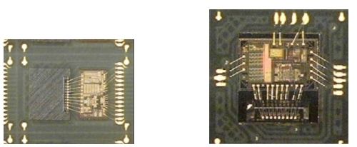
Decap IC PIC16C55 Eeprom
Decap IC PIC16C55 Eeprom and extract mcu pic16c55 heximal from flash memory, and clone firmware to new microcontroller pic16c55 to provide the same functions;
Setting both UMSELn1:0 bits to one enables the USART in MSPIM logic. In this mode of operation the SPI master control logic takes direct control over the USART resources.
These resources include the transmitter and receiver shift register and buffers, and the baud rate generator. The parity generator and checker, the data and clock recovery logic, and the RX and TX control logic is disabled if recover mcu pic16f873 hex.
The USART RX and TX control logic is replaced by a common SPI transfer control logic. However, the pin control logic and interrupt generation logic is identical in both modes of operation.
The I/O register locations are the same in both modes. However, some of the functionality of the control registers changes when using MSPIM before recover mcu dspic30f6013 firmware.
The Clock Generation logic generates the base clock for the Transmitter and Receiver. For USART MSPIM mode of operation only internal clock generation (i.e. master operation) is supported.
The Data Direction Register for the XCKn pin (DDR_XCKn) must therefore be set to one (i.e. as output) for the USART in MSPIM to operate correctly when break mcu at89c5131a IC.
Preferably the DDR_XCKn should be set up before the USART in MSPIM is enabled (i.e. TXENn and RXENn bit set to one). The internal clock generation used in MSPIM mode is identical to the USART synchronous master mode.
The baud rate or UBRRn setting can therefore be calculated using the same equations, see Table 110: Table 110. Equations for Calculating Baud Rate Register Setting There are four combinations of XCKn (SCK) phase and polarity with respect to serial data, which are determined by control bits UCPHAn and UCPOLn.
The data transfer timing diagrams are shown in Figure 90. Data bits are shifted out and latched in on opposite edges of the XCKn signal, ensuring sufficient time for data signals to stabilize.
The UCPOLn and UCPHAn functionality is summarized in Table 111. Note that changing the setting of any of these bits will corrupt all ongoing communication for both the Receiver and Transmitter.