Posts Tagged ‘copy mcu locked content’
 Copy MCU XC18V04PC44C Program
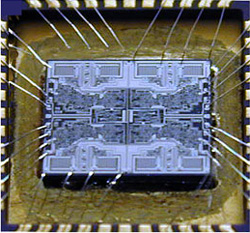
Copy MCU XC18V04PC44C Program
We can Copy MCU XC18V04PC44C Program, please view below MCU XC18V04PC44C features for your reference:
XC18V00 Series In-System-Programmable Configuration PROMs:
Product Specification:
In-System Programmable 3.3V PROMs for Configuration of Xilinx FPGAs
♦ Endurance of 20,000 Program/Erase Cycles
♦ Program/Erase Over Full Industrial Voltage and Temperature Range (–40°C to +85°C)
IEEE Std 1149.1 Boundary-Scan (JTAG) Support
JTAG Command Initiation of Standard FPGA Configuration
Simple Interface to the FPGA
Cascadable for Storing Longer or Multiple Bitstreams
Low-Power Advanced CMOS FLASH Process Dual Configuration Modes
♦ Serial Slow/Fast Configuration (up to 33 MHz)
♦ Parallel (up to 264 Mb/s at 33 MHz)
5V-Tolerant I/O Pins Accept 5V, 3.3V and 2.5V Signals
3.3V or 2.5V Output Capability
Design Support Using the Xilinx ISE™ Foundation™ Software Packages
Available in PC20, SO20, PC44, and VQ44 Packages
Lead-Free (Pb-Free) Packaging
Description
Xilinx introduces the XC18V00 series of in-system programmable configuration PROMs (Figure 1). Devices in this 3.3V family include a 4-megabit, a 2-megabit, a 1-megabit, and a 512-kilobit PROM that provide an easy-to- use, cost-effective method for reprogramming and storing Xilinx FPGA configuration bitstreams. When the FPGA is in Master Serial mode, it generates a configuration clock that drives the PROM.
A short access time after CE and OE are enabled, data is available on the PROM DATA (D0) pin that is connected to the FPGA DIN pin. New data is available a short access time after each rising clock edge. The FPGA generates the appropriate number of clock pulses to complete the configuration. When the FPGA is in Slave Serial mode, the PROM and the FPGA are clocked by an external clock.
When the FPGA is in Master SelectMAP mode, the FPGA generates a configuration clock that drives the PROM. When the FPGA is in Slave Parallel or Slave SelectMAP mode, an external oscillator generates the configuration clock that drives the PROM and the FPGA.
After CE and OE are enabled, data is available on the PROM’s DATA (D0-D7) pins. New data is available a short access time after each rising clock edge. The data is clocked into the FPGA on the following rising edge of the CCLK. A free-running oscillator can be used in the Slave Parallel or Slave SelecMAP modes.
Multiple devices can be cascaded by using the CEO output to drive the CE input of the following device. The clock inputs and the DATA outputs of all PROMs in this chain are interconnected. All devices are compatible and can be cascaded with other members of the family or with the XC17V00 one-time programmable serial PROM family.
Copy MCU ATmega32A Software
Copy MCU ATmega32A Software from master microcontroller ATmega32A program memory, and reprogramme the firmware into blank new Microprocessor ATmega32A for MCU cloning;
Copy MCU ATmega32A Software from master microcontroller ATmega32A program memory, and reprogramme the firmware into blank new Microprocessor ATmega32A for MCU cloning
Features
· High-performance, Low-power AVR® 8-bit Microcontroller
· Advanced RISC Architecture
– 131 Powerful Instructions – Most Single-clock Cycle Execution
– 32 x 8 General Purpose Working Registers
– Fully Static Operation
– Up to 16 MIPS Throughput at 16 MHz
– On-chip 2-cycle Multiplier
High Endurance Non-volatile Memory segments
– 32K Bytes of In-System Self-programmable Flash program memory after firmware MCU PIC16F84 extraction
– 1024 Bytes EEPROM
– 2K Byte Internal SRAM
– Write/Erase Cycles: 10,000 Flash/100,000 EEPROM
– Data retention: 20 years at 85°C/100 years at 25°C(1)
– Optional Boot Code Section with Independent Lock Bits
· In-System Programming by On-chip Boot Program
· True Read-While-Write Operation
– Programming Lock for Software Security
JTAG (IEEE std. 1149.1 Compliant) Interface
– Boundary-scan Capabilities According to the JTAG Standard
– Extensive On-chip Debug Support
– Programming of Flash, EEPROM, Fuses, and Lock Bits through the JTAG Interface
Peripheral Features
– Two 8-bit Timer/Counters with Separate Prescalers and Compare Modes
– One 16-bit Timer/Counter with Separate Prescaler, Compare Mode, and Capture Mode
– Real Time Counter with Separate Oscillator
– Four PWM Channels
– 8-channel, 10-bit ADC
· 8 Single-ended Channels
· 7 Differential Channels in TQFP Package Only
· 2 Differential Channels with Programmable Gain at 1x, 10x, or 200x
– Byte-oriented Two-wire Serial Interface
– Programmable Serial USART
– Master/Slave SPI Serial Interface
– Programmable Watchdog Timer with Separate On-chip Oscillator
– On-chip Analog Comparator
Special Microcontroller Features
– Power-on Reset and Programmable Brown-out Detection
– Internal Calibrated RC Oscillator
– External and Internal Interrupt Sources
– Six Sleep Modes: Idle, ADC Noise Reduction, Power-save, Power-down, Standby and Extended Standby
I/O and Packages
– 32 Programmable I/O Lines
– 40-pin PDIP, 44-lead TQFP, and 44-pad QFN/MLF
Operating Voltages
– 2.7 – 5.5V for ATmega32A
Speed Grades
– 0 – 16 MHz for ATmega32A
Power Consumption at 1 MHz, 3V, 25°C for ATmega32A
Summary
– Active: 0.6 mA
– Idle Mode: 0.2 mA
– Power-down Mode: < 1 µA
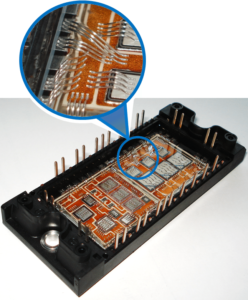
Copy MCU PIC32MX440F512H Binary
Copy MCU PIC32MX440F512H Binary and rewrite the firmware from master Microcontroller PIC32MX440F512H to blank new Microprocessor, decapsulate the MCU PIC32MX440F512H and get access to the databus is the first step of MCU cracking;
High-Performance 32-bit RISC CPU:
· MIPS32® M4K® 32-bit core with 5-stage pipeline
· 80 MHz maximum frequency
· 1.56 DMIPS/MHz (Dhrystone 2.1) performance at 0 wait state Flash access
· Single-cycle multiply and high-performance divide unit
· MIPS16e® mode for up to 40% smaller code size
· Two sets of 32 core register files (32-bit) to reduce interrupt latency
· Prefetch Cache module to speed execution
· Operating temperature range of -40ºC to +105ºC
· Operating voltage range of 2.3V to 3.6V
· 32K to 512K Flash memory (plus an additional 12 KB of boot Flash)
· 8K to 32K SRAM memory
· Pin-compatible with most PIC24/dsPIC® DSC devices
· Multiple power management modes
· Multiple interrupt vectors with individually programmable priority
· Fail-Safe Clock Monitor Mode
· Configurable Watchdog Timer with on-chip Low-Power RC Oscillator for reliable operation
Peripheral Features:
· Atomic SET, CLEAR and INVERT operation on select peripheral registers
· Up to 4-channel hardware DMA with automatic data size detection
· USB 2.0-compliant full-speed device and On-The-Go (OTG) controller
· USB has a dedicated DMA channel
· 3 MHz to 25 MHz crystal oscillator
· Internal 8 MHz and 32 kHz oscillators
· Separate PLLs for CPU and USB clocks
· Two I2C™ modules
· Two UART modules with:
– RS-232, RS-485 and LIN support
– IrDA® with on-chip hardware encoder and decoder
· Up to two SPI modules
· Parallel Master and Slave Port (PMP/PSP) with 8-bit and 16-bit data and up to 16 address lines
· Hardware Real-Time Clock and Calendar (RTCC)
· Five 16-bit Timers/Counters (two 16-bit pairs combine to create two 32-bit timers)
· Five capture inputs
· Five compare/PWM outputs
· Five external interrupt pins
· High-Speed I/O pins capable of toggling at up to 80 MHz
· High-current sink/source (18 mA/18 mA) on all I/O pins
· Configurable open-drain output on digital I/O pins
Debug Features:
· Two programming and debugging Interfaces:
– 2-wire interface with unintrusive access and real-time data exchange with application
– 4-wire MIPS® standard enhanced JTAG interface
· Unintrusive hardware-based instruction trace
· IEEE Standard 1149.2-compatible (JTAG) boundary scan
Analog Features:
· Up to 16-channel 10-bit Analog-to-Digital Converter:
– 1000 ksps conversion rate
– Conversion available during Sleep, Idle
· Two Analog Comparators