 Reverse Engineering Microcontroller ATMEGA2560V Firmware
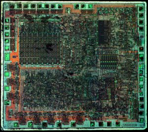
We can Reverse engineering Microcontroller ATMEGA2560V Firmware, please view the Microcontroller ATMEGA2560V features for your reference:
The ATmega2560v implements 256 bytes of RAM. The upper 128 bytes of RAM occupy a parallel space to the Special Function Registers. That means the upper 128 bytes have the same addresses as the SFR space but are physically separate from SFR space.
When an instruction accesses an internal location above address 7FH, the address mode used in the instruction specifies whether the CPU accesses the upper 128 bytes of RAM or the SFR space. Instructions that use direct addressing access SFR space.
For example, the following direct addressing instruction accesses the SFR at location 0A0H (which is P2). MOV 0A0H, #data
Instructions that use indirect addressing access the upper 128 bytes of RAM. For example, the following indirect addressing instruction, where R0 contains 0A0H, accesses the data byte at address 0A0H, rather than P2 (whose address is 0A0H) before Reverse Engineering Microcontroller ATMEGA2560V Firmware.
Note that stack operations are examples of indirect addressing, so the upper 128 bytes of data RAM are available as stack, The programmable Watchdog Timer (WDT) operates from an independent oscillator. The prescaler bits, PS0, PS1 and PS2 in SFR WCON are used to set the period of the Watchdog Timer from 16 ms to 2048 ms.
The available timer periods are shown in the following table and the actual timer periods (at VCC = 5V) are within ±30% of the nominal. The WDT is disabled by Power-on Reset and during Power Down. It is enabled by setting the WDTEN bit in SFR WCON (address = 96H) after Reverse Engineering Microcontroller ATMEGA2560V Firmware.
The WDT is reset by setting the WDTRST bit in WCON. When the WDT times out without being reset or disabled, an internal RST pulse is generated to reset the CPU. Table 7. Watchdog Timer Period Selection space.
Timer 0 and Timer 1 in the AT89LS53 operate the same way as Timer 0 and Timer 1 in the AT89C51, AT89C52 and AT89C55. For further information, see the October 1995 Microcontroller Data Book, page 2-45, section titled, “Timer/Counters.”
Timer 2 is a 16 bit Timer/Counter that can operate as either a timer or an event counter. The type of operation is selected by bit C/T2 in the SFR T2CON (shown in Table 2). Timer 2 has three operating modes: capture, auto-reload (up or down counting), and baud rate generator before Reverse Engineering Microcontroller ATMEGA2560V Firmware.
The modes are selected by bits in T2CON, as shown in Table 8. Timer 2 consists of two 8-bit registers, TH2 and TL2. In the Timer function, the TL2 register is incremented every machine cycle. Since a machine cycle consists of 12 oscillator periods, the count rate is 1/12 of the oscillator frequency.
In the Counter function, the register is incremented in response to a 1-to-0 transition at its corresponding external input pin, T2. In this function, the external input is sampled during S5P2 of every machine cycle. When the samples show a high in one cycle and a low in the next cycle, the count is incremented.
The new count value appears in the register during S3P1 of the cycle following the one in which the transition was detected. Since two machine cycles (24 oscillator periods) are required to recognize a 1-to-0 transition, the maximum count rate is 1/24 of the oscillator frequency. To ensure that a given level is sampled at least once before it changes, the level should be held for at least one full machine cycle when Reverse Engineering Microcontroller ATMEGA2560V Firmware.