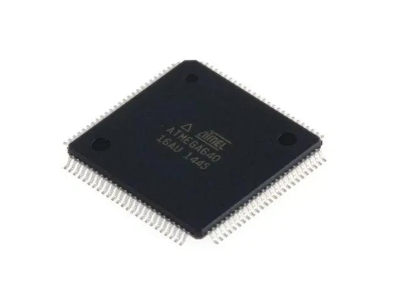
 Reverse Engineering MCU ATMEGA640P Flash
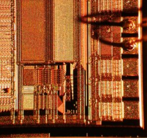
Reverse Engineering MCU ATmega640P to figure out the location of security fuse bit of Microcontroller ATmega640P by MCU cracking technique, then extract code from microcontroller ATmega640P Flash memory;
Reverse Engineering MCU ATMEGA640P to figure out the location of security fuse bit of Microcontroller ATmega640P by MCU cracking technique, then extract code
The Compare Output mode (COM0x1:0) bits have two functions. The Waveform Generator uses the COM0x1:0 bits for defining the Output Compare (OC0x) state at the next Compare Match. Also, the COM0x1:0 bits control the OC0x pin output source. Figure 41 shows a simplified schematic of the logic affected by the COM0x1:0 bit setting if MCU ATmega644 code recovering.
The I/O Registers, I/O bits, and I/O pins in the figure are shown in bold. Only the parts of the general I/O Port Control Registers (DDR and PORT) that are affected by the COM0x1:0 bits are shown. When referring to the OC0x state, the reference is for the internal OC0x Register, not the OC0x pin. If a system reset occur, the OC0x Register is reset to “0”.
The general I/O port function is overridden by the Output Compare (OC0x) from the Waveform Generator if either of the COM0x1:0 bits are set. However, the OC0x pin direction (input or output) is still controlled by the Data Direction Register (DDR) for the port pin. The Data Direction Register bit for the OC0x pin (DDR_OC0x) must be set as output before the OC0x value is visible on the pin. The port override function is independent of the Waveform Generation mode.
unlock ATMEGA640A atmel microprocessor secured and recover embedded heximal data from flash memory
The design of the Output Compare pin logic allows initialization of the OC0x state before the output is enabled. Note that some COM0x1:0 bit settings are reserved for certain modes of operation. See “8-bit Timer/Counter Register Description”.
The Waveform Generator uses the COM0x1:0 bits differently in Normal, CTC, and PWM modes. For all modes, setting the COM0x1:0 = 0 tells the Waveform Generator that no action on the OC0x Register is to be performed on the next Compare Match.
For compare output actions in the non-PWM modes refer to Table 70 on page 128. For fast PWM mode, refer to Table 71 on page 128, and for phase correct PWM refer to Table 72 on page 129. A change of the COM0x1:0 bits state will have effect at the first Compare Match after the bits are written. For non-PWM modes, the action can be forced to have immediate effect by using the FOC0x strobe bits.