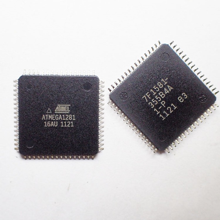
 Reverse Engineering MCU ATmega1281P Firmware
Reverse Engineering MCU ATmega1281P and copy embedded Firmware from microcontroller atmega1281p memory to new MCU, to make microprocessor atmega1281p cloning units.
The Timer/Counter Overflow Flag (TOVn) is set at the same timer clock cycle as the OCRnx Registers are updated with the double buffer value (at BOTTOM).
When either OCRnA or ICRn is used for defining the TOP value, the OCnA or ICFn Flag set when TCNTn has reached TOP. The Interrupt Flags can then be used to generate an interrupt each time the counter reaches the TOP or BOTTOM value.
When changing the TOP value the program must ensure that the new TOP value is higher or equal to the value of all of the Compare Registers. If the TOP value is lower than any of the Compare Registers, a compare match will never occur between the TCNTn and the OCRnx before attack microcontroller mc68hc705p6a memory.
As Figure 57 shows the output generated is, in contrast to the phase correct mode, symmetrical in all periods. Since the OCRnx Registers are updated at BOTTOM, the length of the rising and the falling slopes will always be equal. This gives symmetrical output pulses and is therefore frequency correct.
Using the ICRn Register for defining TOP works well when using fixed TOP values. By using ICRn, the OCRnA Register is free to be used for generating a PWM output on OCnA before copying pic16lf877 MCU program.
However, if the base PWM frequency is actively changed by changing the TOP value, using the OCRnA as TOP is clearly a better choice due to its double buffer feature.
In phase and frequency correct PWM mode, the compare units allow generation of PWM waveforms on the OCnx pins. Setting the COMnx1:0 bits to two will produce a non-inverted PWM and an inverted PWM output can be generated by setting the COMnx1:0 to three.
crack locked microcontroller ATMEGA1281 memory and clone its heximal file from program flash and data eeprom
The actual OCnx value will only be visible on the port pin if the data direction for the port pin is set as output (DDR_OCnx). The PWM waveform is generated by setting (or clearing) the OCnx Register at the compare match between OCRnx and TCNTn when the counter increments, and clearing (or setting) the OCnx Register at compare match between OCRnx and TCNTn when the counter decrements.
The PWM frequency for the output when using phase and frequency correct PWM can be calculated by the following equation:
The N variable represents the prescaler divider (1, 8, 64, 256, or 1024). The extreme values for the OCRnx Register represents special cases when generating a PWM waveform output in the phase correct PWM mode.
If the OCRnx is set equal to BOTTOM the output will be continuously low and if set equal to TOP the output will be set to high for non-inverted PWM mode. For inverted PWM the output will have the opposite logic values. If OCR1A is used to define the TOP value (WGM13:0 = 9) and COM1A1:0 = 1, the OC1A output will toggle with a 50% duty cycle.