 Reverse Engineering IC ATmega644A Firmware
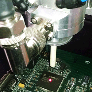
Reverse Engineering IC ATmega644A and clone ATmega644A microcontroller firmware from embedded flash and eeprom memory;
If the On-chip debug system is enabled by the OCDEN Fuse and the chip enters sleep mode, the main clock source is enabled, and hence, always consumes power. In the deeper sleep modes, this will contribute significantly to the total current consumption.
There are three alternative ways to disable the OCD system: Disable the OCDEN Fuse. Disable the JTAGEN Fuse. Write one to the JTD bit in MCUCR.
During reset, all I/O Registers are set to their initial values, and the program starts execution from the Reset Vector. The instruction placed at the Reset Vector must be a JMP – Absolute Jump – instruction to the reset handling routine.
If the program never enables an interrupt source, the Interrupt Vectors are not used, and regular program firmware can be placed at these locations. This is also the case if the Reset Vector is in the Application section while the Interrupt Vectors are in the Boot section or vice versa before attack microcontroller mc68hc705p6 bin.
The circuit diagram in Figure 25 shows the reset logic. Table 23 defines the electrical parameters of the reset circuitry. The I/O ports of the AVR are immediately reset to their initial state when a reset source goes active. This does not require any clock source to be running if attack chip st62t00cb6 firmware.
After all reset sources have gone inactive, a delay counter is invoked, stretching the internal reset. This allows the power to reach a stable level before normal operation starts. The time-out period of the delay counter is defined by the user through the SUT and CKSEL Fuses. The different selections for the delay period are presented in “Clock Sources”.
The ATmega644 has five sources of reset: Power-on Reset. The MCU is reset when the supply voltage is below the Power-on Reset threshold (VPOT). External Reset. The MCU is reset when a low level is present on the RESET pin for longer than the minimum pulse length before copy mcu pic18f2480 program.
Watchdog Reset. The MCU is reset when the Watchdog Timer period expires and the Watchdog is enabled. Brown-out Reset. The MCU is reset when the supply voltage VCC is below the Brown-out Reset threshold (VBOT) and the Brown-out Detector is enabled.
JTAG AVR Reset. The MCU is reset as long as there is a logic one in the Reset Register, one of the scan chains of the JTAG system. Refer to the section “IEEE 1149.1 (JTAG) Boundary-scan” on page 301 for details.
A Power-on Reset (POR) pulse is generated by an On-chip detection circuit. The detection level is defined in Table 23. The POR is activated whenever VCC is below the detection level. The POR circuit can be used to trigger the start-up Reset, as well as to detect a failure in supply voltage.
A Power-on Reset (POR) circuit ensures that the device is reset from Power-on. Reaching the Power-on Reset threshold voltage invokes the delay counter, which determines how long the device is kept in RESET after VCC rise. The RESET signal is activated again, without any delay, when VCC decreases below the detection level.
An External Reset is generated by a low level on the RESET pin. Reset pulses longer than the minimum pulse width (see Table 23) will generate a reset, even if the clock is not running. Shorter pulses are not guaranteed to generate a reset. When the applied signal reaches the Reset Threshold Voltage – VRST – on its positive edge, the delay counter starts the MCU after the Time-out period – tTOUT – has expired.
ATmega644 has an On-chip Brown-out Detection (BOD) circuit for monitoring the VCC level during operation by comparing it to a fixed trigger level. The trigger level for the BOD can be selected by the BODLEVEL Fuses. The trigger level has a hysteresis to ensure spike free Brown-out Detection. The hysteresis on the detection level should be interpreted as VBOT+ = VBOT + VHYST/2 and VBOT- = VBOT – VHYST/2.