 Recover MCU PIC16HV616 Eeprom
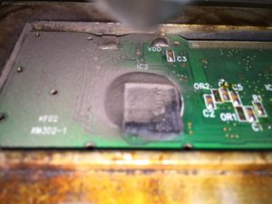
Recover MCU PIC16HV616 Eeprom content needs to crack microcomputer chip pic16hv616 and readout the embedded heximal from microcontroller pic16hv616 flash memory;
The data memory (see Figure 2-4) is partitioned into two banks, which contain the General Purpose Registers (GPR) and the Special Function Registers (SFR). The Special Function Registers are located in the first 32 locations of each bank.
PIC16F610/16HV610 Register locations 40h-7Fh in Bank 0 are General Purpose Registers, implemented as static RAM. PIC16F616/16HV616 Register locations 20h-7Fh in Bank 0 and A0h-BFh in Bank 1 are General Purpose Registers, implemented as static RAM. Register locations F0h-FFh in Bank 1 point to addresses 70h-7Fh in Bank 0. All other RAM is unimplemented and returns ‘0’ when read. The RP0 bit of the STATUS register is the bank select bit.
The register file is organized as 64 x 8 in the PIC16F610/16HV610 and 128 x 8 in the PIC16F616/16HV616. Each register is accessed, either directly or indirectly, through the File Select Register (FSR) (see Section 2.4 “Indirect Addressing, INDF and FSR Registers”) if copy pic16c72 Mcu software.
The Special Function Registers are registers used by the CPU and peripheral functions for controlling the desired operation of the device (see Table 2-1). These registers are static RAM. The special registers can be classified into two sets: core and peripheral. The Special Function Registers associated with the “core” are described in this section. Those related to the operation of the peripheral features are described in the section of that peripheral feature.
The STATUS register, shown in Register 2-1, contains:
· the arithmetic status of the ALU
· the Reset status
· the bank select bits for data memory (RAM)
The STATUS register can be the destination for any instruction, like any other register. If the STATUS register is the destination for an instruction that affects the Z, DC or C bits, then the write to these three bits is disabled. These bits are set or cleared according to the device logic. Furthermore, the TO and PD bits are not writable. Therefore, the result of an instruction with the STATUS register as destination may be different than intended.
For example, CLRF STATUS, will clear the upper three bits and set the Z bit. This leaves the STATUS register as ‘000u u1uu’ (where u = unchanged). The Program Counter (PC) is 13 bits wide. The low byte comes from the PCL register, which is a readable and writable register. The high byte (PC<12:8>) is not directly readable or writable and comes from PCLATH. On any Reset, the PC is cleared.
Figure 2-5 shows the two situations for the loading of the PC. The upper example in Figure 2-5 shows how the PC is loaded on a write to PCL (PCLATH<4:0> → PCH). The lower example in Figure 2-5 shows how the PC is loaded during aCALL or GOTO instruction (PCLATH<4:3> → PCH).