 Recover MCU ATtiny261V Code
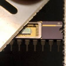
Recover MCU ATtiny261V Code from secured memory, the fuse bit of microcontroller attiny261v will be cracked to reset the status of flash and eeprom memory, program and data in the format of heximal can be extracted from mcu attiny261v and copy to new MCU;
The AVR core combines a rich instruction set with 32 general purpose working registers. All the 32 registers are directly connected to the Arithmetic Logic Unit (ALU), allowing two independent registers to be accessed in one single instruction executed in one clock cycle.
The resulting architecture is more code efficient while achieving throughputs up to ten times faster than conventional CISC microcontrollers if copy pic16f870 MCU program.
The ATtiny261/461/861 provides the following features: 2/4/8K byte of In-System Programmable Flash, 128/256/512 bytes EEPROM, 128/256/512 bytes SRAM, 6 general purpose I/O lines, 32 general purpose working registers, one 8-bit Timer/Counter with compare modes, one 8-bit high speed Timer/Counter, Universal Serial Interface, Internal and External Interrupts, a 4-channel, 10-bit ADC, a programmable Watchdog Timer with internal Oscillator, and three software selectable power saving modes.
The Idle mode stops the CPU while allowing the SRAM, Timer/Counter, ADC, Analog Comparator, and Interrupt system to continue functioning.
The Power-down mode saves the register contents, disabling all chip functions until the next Interrupt or Hardware Reset. The ADC Noise Reduction mode stops the CPU and all I/O modules except ADC, to minimize switching noise during ADC conversions after break pic18f8722 MCU flash content.
The device is manufactured using Atmel’s high density non-volatile memory technology. The On-chip ISP Flash allows the Program memory to be re-programmed In-System through an SPI serial interface, by a conventional non-volatile memory programmer or by an On-chip boot code running on the AVR core.
The ATtiny261/461/861 AVR is supported with a full suite of program and system development tools including: C Compilers, Macro Assemblers, Program Debugger/Simulators, In-Circuit Emulators, and Evaluation kits.
Port A is an 8-bit bi-directional I/O port with internal pull-up resistors (selected for each bit). The Port A output buffers have symmetrical drive characteristics with both high sink and source capability.
As inputs, Port A pins that are externally pulled low will source current if the pull-up resistors are activated. The Port A pins are tri-stated when a reset condition becomes active, even if the clock is not running after Recover MCU.
Port B is an 8-bit bi-directional I/O port with internal pull-up resistors (selected for each bit). The Port B output buffers have symmetrical drive characteristics with both high sink and source capability.
As inputs, Port B pins that are externally pulled low will source current if the pull-up resistors are activated. The Port B pins are tri-stated when a reset condition becomes active, even if the clock is not running.
For compatibility with future devices, reserved bits should be written to zero if accessed. Reserved I/O memory addresses should never be written.
I/O Registers within the address range 0x00 – 0x1F are directly bit-accessible using the SBI and CBI instructions. In these registers, the value of single bits can be checked by using the SBIS and SBIC instructions.
Some of the Status Flags are cleared by writing a logical one to them. Note that, unlike most other AVRs, the CBI and SBI instructions will only operation the specified bit, and can therefore be used on registers containing such Status Flags. The CBI and SBI instructions work with registers 0x00 to 0x1F only.