 Recover Chip MC68HC11A0FN3 Binary
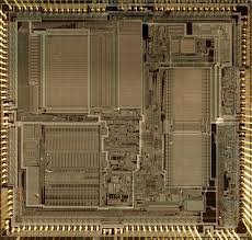
Recover Chip MC68HC11A0FN3 Binary from Microcontroller MC68HC11A0FN3 program memory, unlock microprocessor MC68HC11A0FN3 security fuse bit and extract heximal out from memory
Recover Chip MC68HC11A0FN3 Binary from Microcontroller MC68HC11A0FN3 program memory, unlock microprocessor MC68HC11A0FN3 security fuse bit and extract heximal out from memory;
· Power Saving STOP and WAIT Modes
· 4 Kbytes of On-Chip ROM
· 192 Bytes of On-Chip RAM (All Saved During Standby)
· 16-Bit Timer System
— 3 Input Capture (IC) Channels
— 4 Output Compare (OC) Channels
— One IC or OC Channel (Software Selectable)
· 8-Bit Pulse Accumulator
· Real-Time Interrupt Circuit
· Computer Operating Properly (COP) Watchdog System
· Synchronous Serial Peripheral Interface (SPI)
· Asynchronous Nonreturn to Zero (NRZ) Serial Communications Interface (SCI)
· 26 Input/Output (I/O) Pins
— 16 Bidirectional I/O Pins
— 3 Input Only Pins
— 3 Output Only Pins (One Output Only Pin in the 40-Pin Package)
· Available in a 44-Pin Plastic Leaded Chip Carrier (PLCC) and 40-Pin Dual In-Line Package (DIP)
2.1 VDD, VSS, and EVSS
Power is supplied to the MCU through VDD and VSS. VSS is the power supply, and VSS is ground. EVSS, available on the 44-pin PLCC, is an additional ground pin that must be grounded with VSS. The MCU operates from a single 5-volt (nominal) power supply before MCU PIC32MX440F512H binary copying. Very fast signal transitions occur on the MCU pins.
The short rise and fall times place high, short duration current demands on the power supply. To prevent noise problems, provide good power supply bypassing at the MCU. Also, use bypass capacitors that have good high-frequency characteristics and situate them as close to the MCU as possible. Bypass requirements vary, depending on how heavily the MCU pins are loaded.
2.2 Reset (RESET)
An active low bidirectional control signal, RESET, acts as an input to initialize the MCU to a known startup state. It also acts as an open-drain output to indicate that an internal failure has been detected in either the clock monitor or COP watchdog circuit. The CPU distinguishes between internal and external reset conditions by sensing whether the reset pin rises to a logic one in less than two E-clock cycles after a reset has occurred. It is not advisable to connect an external resistor-capacitor (RC) power-up delay circuit to the reset pin of M68HC11 devices because the circuit charge time.
2.3 Crystal Driver and External Clock Input (XTAL, EXTAL)
These two pins provide the interface for either a crystal or a CMOS compatible clock to control the internal clock generator circuitry. The frequency applied to these pins is four times higher than the desired E-clock rate after Recover MCU PIC16F913 bin.
The XTAL pin is normally left unterminated when an external CMOS compatible clock input is connected to the EXTAL pin. However, a 10 kΩ to 100 kΩ load resistor connected from XTAL to ground can be used to reduce RFI noise emission. The XTAL output is normally intended to drive only a crystal. The XTAL output can be buffered with a high impedance buffer, or it can be used to drive the EXTAL input of another M68HC11.