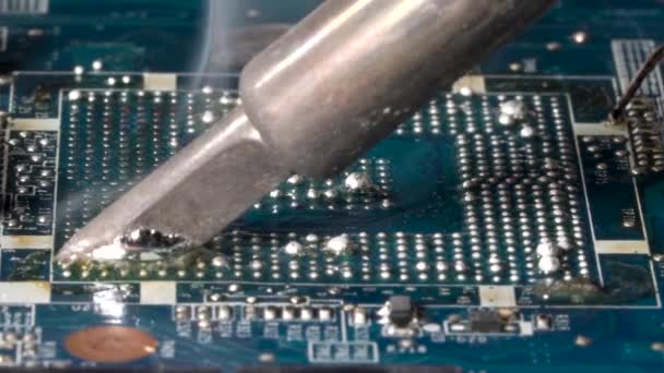
 PCB Relayout Capabilities
PCB Relayout can also be defined as circuit board schematic diagram modification through which the electrical and electronic performance of printed circuit board will be improved;

—- We can handle single sided, double sided, multilayer up to 20 layers PCB Relayout;
—- No limit on nodes, holes and pads, holes refers to PCB Board with Blind & Buried via down to 0.1mm;
—- Circuit Board size range from 546*622mm due to the capability limitation, over that size;
—- No limitation on components type (through hole, surface mount, or mixed);
—- SMT pitch down to 0.2mm or less depending on board layout;
—- Application refers to Measurement, Telecommunication, Networking, Consumer Electronics, Industrial Automation;
Service Deliver:
We can send your emails containing all the information and files you need to remanufacture your electronic PCB card:
1 Schematic diagrams and drawing files; (Optional)
2 Bill of materials (BOM) list all components as well as individual description;
3 PCB plate Gerber files and drilling/outline files for the prototype or mass production;
4 Optional: A fully functional prototype PCB Assembled with all components as-specified for testing and evaluation.
There may be noticeably a bundle to know about this. I assume you made certain good factors in features also.
hgh Hello
5