 Decode Locked MCU PIC16F57 Heximal Data
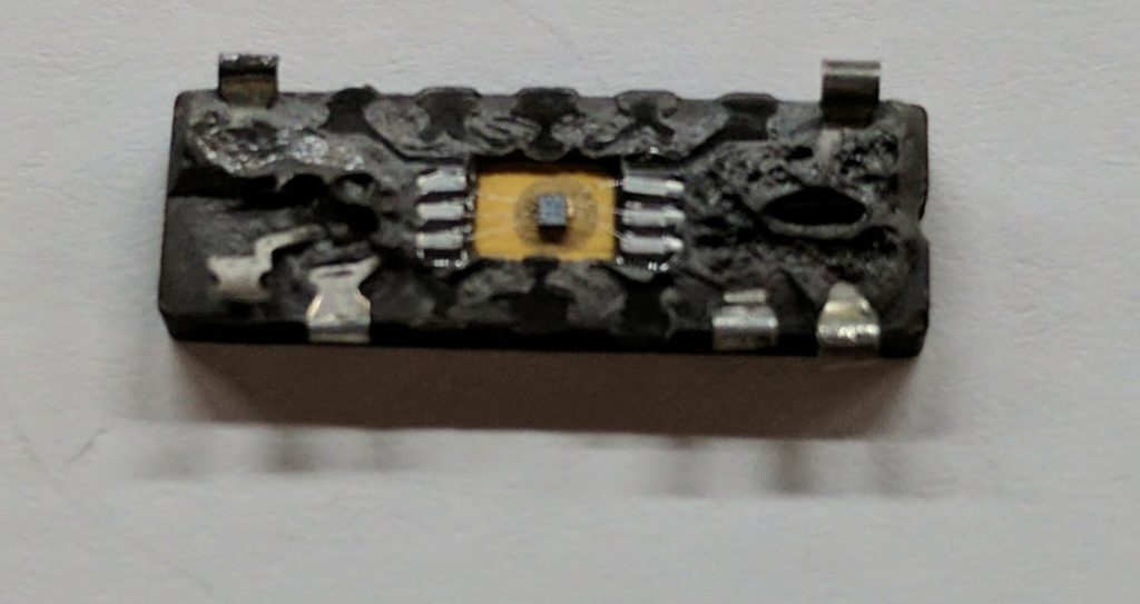
Decode Locked MCU PIC16F57 Heximal Data from eeprom memory, unlock microcontroller PIC16F57 security fuse bit and extract firmware out from microprocessor memory;
The Timer0 module has the following features:
8-bit timer/counter register, TMR0
– Readable and writable
8-bit heximal data programmable prescaler
Internal or external clock select
– Edge select for external clock
Figure 6-1 is a simplified block diagram of the Timer0 module.
Timer mode is selected by clearing the T0CS bit (OPTION<5>). In timer mode, the Timer0 module will increment every instruction cycle (without prescaler) if break ic pic16f917 hex.
If TMR0 register is written, the increment is inhibited for the following two instruction cycles (Figure 6-2 and Figure 6-3). The user can work around this by writing an adjusted value to the TMR0 register.
Counter mode is selected by setting the T0CS bit (OPTION<5>). In this mode, Timer0 will increment either on every rising or falling edge of pin T0CKI.
The T0SE bit (OPTION<4>) determines the source edge. Clearing the T0SE bit selects the rising edge. Restrictions on the external clock input are discussed in detail in Section 6.1.
The prescaler may be used by either the Timer0 module or the Watchdog Timer, but not both. The prescaler assignment is controlled in heximal data by the control bit PSA (OPTION<3>) after recover mcu pic16f72 code.
Clearing the PSA bit will assign the prescaler to Timer0. The prescaler is not readable or writable. When the prescaler is assigned to the Timer0 module, prescale values of 1:2, 1:4,…, 1:256 are selectable. Section 6.2 details the operation of the prescaler.
A summary of registers associated with the Timer0 When an external clock input is used for Timer0, it must meet certain requirements. The external clock requirement is due to internal phase clock (TOSC) synchronization when recover mcu pic16f77 eeprom.
Also, there is a delay in the actual incrementing of Timer0 after synchronization. When no prescaler is used, the external clock input is the same as the prescaler output.
The synchronization of T0CKI with the internal phase clocks is accomplished by sampling the prescaler output on the Q2 and Q4 cycles of the internal phase clocks. Therefore, it is necessary for T0CKI to be high for at least 2TOSC (and a small RC delay of 20 ns) and low for at least 2TOSC (and a small RC delay of 20 ns). Refer to the electrical specification of the desired device.