Archive for the ‘PCB Design’ Category
 Increase radiation heat dissipation can apply below methods
1> Apply material which has large emitting and absorbing features;
2> Increase the temperature of radiated article;
3> Decrease the temperature of absorbing article;
Heat dissipation through convection can be realized through below ways
1> Increase the surface size to speed up heat dissipation;
2> Increase heat dissipation efficiency by replacing layer flow by interference flow;
3> Ensure the rounding environment of part where need to cooling can tidy up;
Heat dissipation through thermal conductance can be realized through below ways
1> Use high heat conducting material;
2> Keep distance from heat source to heat dissipation the shortest way;
3> Ensure stable heat connecting among each conducting routes;
4> Install as large printed circuit conductor as possible in the route of heat dissipation;
Hole diameter of PAD when design a printed circuit board
In order to achieve the minimum diameter when design PCB according to the requirement of PAD, the diameter at least should be 0.5mmlarger than maximum diameter of soldering pin outer flange.
Designer has to provide testing PAD for all of joints according to ANSI/IPC 2221. JOINT means the electric connection among 2 or above components. One testing PAD need to use one signal node, coordinate location of testing PAD (also need to specify which side the testing PAD at) and X-Y coordinate axis of printed circuit board datum mark. Designer need to provide fixing installation data for SMT, as well as PCB layout technology, through which the testability of circuit diagram can be improved by the assistance of IN-CIRCUIT test fixing installation.
Below conditions are required:
1> Diameter of PAD specify for in-circuit electric testing shouldn’t larger than0.9mm;
2> Space around testing PAD should larger than0.6mmbut smaller than5mm, if the height of component greater than6.7mm, then this testing PAD should be placed5mmaway from this component;
3> No components or testing PAD would be allowed to placed within3mmarea;
4> Testing PAD should be placed in the center of2.5mmdiameter, if possible, apply a standard probe and more reliable fixing device is allowable.
5> Don’t use the edge of connector’s pin to instruct PAD testing, since the testing probe could readily damage the gold-plated pins.
Aspect ratio of plated-through hole has great impact on effectively through-hole plating capability for manufacturer, it is also very critical for ensuring the structure of PTH/PTV. When the diameter of hole smaller than 1/4 of basic printed circuit board thickness, tolerance should increase0.05mm. When drilling hole diameter is0.35mmor even smaller, aspect ratio could be 4:1 or even larger, manufacturer should use the proper way to shield or block the through-hole to prevent entering of the solder, generally speaking, printed circuit board thickness and plated through hole ratio should less than 5:1.
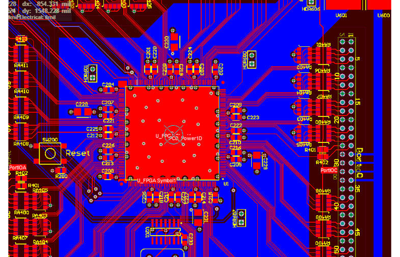
Layout draft of printed circuit board
Layout draft of printed circuit board can describe the final drawing of each components and layout design of interconnected circuit, it can also provide sufficient information for the final prototype drawing. Moreover, layout draft also include component hole, wire width and space.
Before designer begin to make out plan for printed circuit board layout draft, we suggest to prepare a trial draft, also takes below factors into consideration:
1> Size of printed circuit board—depends on the space of equipment or use standard size;
2> Profile of component—attain from data handbook;
3> Installation datasheet of component—if install professional version, need to take data handbook as reference, if has thermal limitation need to use heat-sink or high volume capacitor;
4> Interconnect graphics;
5> Width and space of wire—it depends on the functional requirement of wire;
6> Edge line—Normally will leave 0.5cm for each edge;
7> Connector—Size and type of connector depends on the outer connection, such as power input and output signal, grounding and device requirement.
8> Fixing gadget—screw and clip;
Layout design is always a process of experiment and error-checking, before the final result come out, it need to modify and adjust again and again.
Attentions of Printed circuit board layout design
Hole and PAD on printed circuit board need to array according to standard system, it is more important in multilayer printed circuit board design, because during the process of manufacturing, each layer need to align with other layers. As seen from standard system as picture below, it use 2 mutual related graphics, one is standard or one reference line, as well as standard symbol, all the components array should base upon these symbols. Below factors should be taken into consideration:
1> Fix 0/0 fiducial location, ensure all or most part of printed circuit board could be covered within the area of cartesian coordinate.
2> Fix most of components space and locations, and install the original diagram network. Specify all components which are not suitable for identify in the graphic.
3> Refers to the manufacturing and assembling aspects, we have to consider the locations requirement of holes. If size and density of printed circuit board prohibit add internal hole, then designer has to integrate panel board with external hole and view it as part of design.
Rational installation of power wire ground wire of printed circuit board
Power wire should has enough width to ensure low resistance and small inductance, however, value of capacitance coupling will increase accompany with its width.
On the same printed circuit board, simulated circuit and digital circuit should strictly separated by ground wire network. Moreover, reference voltage normally would be quite sensitive to vibration of ground level, so it should be separated from power wire, connect directly to the incoming interface of printed circuit board, furthermore, its ground wire should connect to an isolated and stable reference ground point of device.
Generally speaking, ground wire not only has resistance, but also inductance, additionally, it will has unknown current pass by, voltage of resistor will decrease when current pass it. CAD program has great number of defects on ground wire design of printed circuit board, because they would design all the wires as thin as they can for the sake of saving more copper size, this will bring much higher ground resistance. The most obvious way to substitute the thin ground wire is connecting all the ground wires on the copper clad layer to form a continual grounding side. Since 0.001inch (0.025mm) copper resistance is around 0.67 mΩ/in2, so under normal circumstance it is enough already.
PCB Circuit Board Schematic Diagram Drawing Process
PCB Circuit Board Schematic Diagram Drawing Process include add the new files, and install working environment, placing electronic components, then layout the schematic diagram:
1 Add new SCH file:
Before entering SCH design system, first you should have general image of the schematic diagram you are about to draw, that is to say you have to understand what circuit need to use on the design of your schematic diagram, and then use PROTEL DXP to draw schematic diagram;
2 Install working environment:
You should choose the right size of drawing paper according to the complexity level of circuit pattern. During the whole process of circuit design, size of drawing paper can be adjusted so set up the proper size of drawing paper could be defined as the 1st step of schematic diagram drawing.
3 Component placement:
Choose components from library, dissipate them onto proper location of drawing and define their name, package method, Adjust and modify the locations of each components according to their electronic connection and circuit relations to make it more reliable and easy to understand.
4 Layout of Schematic Diagram:
Layout schematic diagram according to the requirement of circuit pattern by using different kinds of tools and instruction provide by SCH software, connect all the components on the surface through their electrical connection by circuit and symbol, to form a complete schematic diagram.
Multilayer PCB Board Design Performance Requirement
Design performance of multilayer PCB Board is similar to most of single layer and double layer PCB Board, it can avoid too much circuit fill in the very limited space, lead to impractical tolerance, high inner layer volume, even threaten the safety of product quality. Therefore, performance specification should consider complete evaluation include thermal shock, insulation resistance, resistance welding of inner layer circuit, below content discuss the mainly aspects during the process of multilayer PCB Board design.
1 Mechanical design factors:
Mechanical design include choose appropriate PCB Board dimension, PCB Board thickness, PCB Board lay-up, inner layer copper thickness, aspect ratio.
1> PCB Board Dimension
Dimension should be designed according to application, size of system cabine, production capability limitation of PCB Board manufacturer to choose the optimal selection. Big PCB Board has many advantages, such as less laminate, shorter circuit routes among different components, which will result in higher operation speed, moreover, each PCB Board can have more IN/OUT connection, therefore big PCB Board should be 1st choice among different kinds of application. For instance in the personal computer, most of motherboard we can see are all big PCB Board. However, design signal wire layout is not an easy task, since it needs more signal layer and inner layer connection or space, the difficulty level of heat treatment could be higher too. Designer should take various reasons into account, such as standard board dimension, dimension of manufacture facility and limitation of manufacture process. In IPC-D-322 has listed some guidance about how to choose the right dimension of Printed Circuit Board.
2> PCB Board thickness
Thickness of PCB Board is determined by different elements, such as amount of signal layer, thickness and quantity of power layer, hole quantity and diameter of through-hole as well as aspect ratio, lead length of automatic insert component and connection type. Total thickness of PCB Board is make up of conducting layer, copper layer, base laminate and pre-dip material. It is difficult to control the multilayer PCB Board, so +/-10% tolerance can be viewed as reasonable.
3> Lay-Up Structure
In order to decrease PCB Board twist into the minimum level so can have as flat as possible, the inner layer of multilayer PCB Board should be keep symmetrical. So the copper layer quantity should be even, and ensure copper thickness and copper circuit pattern symmetrical. Generally the material and structure of laminate (such as glass fiber) should parallel with the edge direction of PCB Board. Because after pressing the laminate will constrict which will cause the layout of PCB Board distorted, more liable to variability and low space stability.
However, through improve PCB design can make the bow and twist of multilayer PCB Board to minimum level. Through the dissipation of copper to ensure the structure symmetry, as well as the deep-dip material being separate evenly with reasonable thickness, through which can reach the purpose of decreasing bow and twist. PCB Board manufacture should start right from the core layer, till the outer layer of surface. The minimum thickness among 2 copper layer (dielectric layer) is 0.08mm.
According to the experience, the minimum distance between 2 copper layer, that is presoak material minimum thickness after laminate should at least 2 times of copper thickness. In other words, if the 2 adjacent copper layer thickness is 30μm, so the dielectric material thickness should be at least 2*(2*30μm)=120μm, this thickness will need to 2 piece of 1080 pre-preg material.
4> Inner layer copper
Most frequent used copper is 1oz, however, for the high intensity PCB Board, it is thickness is critical since it will has strictly impedance control. This kind of PCB Board will use 0.5oz copper, for power layer and ground layer, we should choose 2oz or even heavier copper. Etching heavier copper will decrease the controllability, it could bring difficulty to realize the tolerance pattern of circuit width and space. So it need special treatment.
5> Hole
According to the diameter of component lead or dimension of catercorner, plated through hole’s diameter normally remain among 0.028 to 0.01 inch, which can ensure the enough space and better soldering.
6> Aspect Ratio
“Aspect Ratio” is the ratio among PCB Board thickness and hole diameter. Normally speaking 3:1 can be viewed as the standard ratio, although 5:1 is also quite normal. Aspect Ratio can be determined through different elements like drilling, desmear or etch-back and plating.
2 Electric Design
Multilayer PCB Board is a high performance, high speed system. Refers to high frequency, time length of signal increase become shorter, therefore signal reflection and circuit length control become quite important. In the multilayer system, the requirement of component controllable impedance performance is very high, so electric design should follow above requirement. About elements decide the impedance value include laminate and pre-preg material dielectric, wire space of same layer, dielectric thickness and copper conductor thickness. In the high speed application, laminate sequence and signal network connecting sequence are paramount for multilayer PCB Board, dielectric parameter is critical to determine impedance, propagation delay and capacitor. The dielectric of epoxy glass laminate and prepreg can be modified through adjust content level of resin.
Epoxy resin dielectric parameter is 3.45, glass is 6.2. Through control the content level of these material, the dielectric of epoxy-glass can reach 4.2-5.3.
Relative low dielectric of prepreg material is more suitable for radio frequency and microwave circuit. In the radio frequency and microwave, lower dielectric parameter will has less signal propagation delay. In the base laminate, low dissipation factor can make the electric loss reach the minimum level.