Archive for the ‘Break IC’ Category
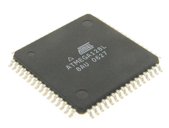
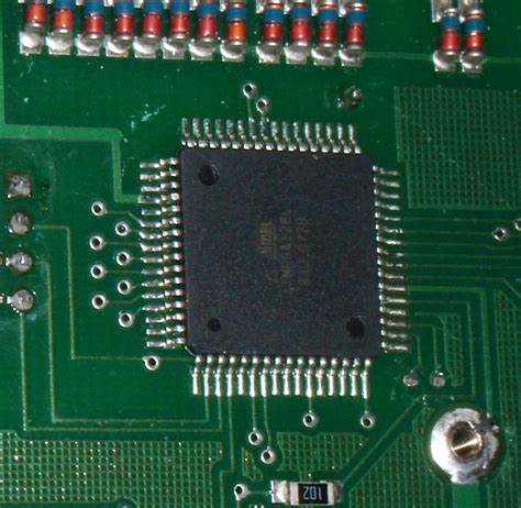
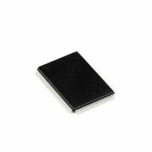
 Crack Locked ATMEGA128L AVR Chip
Crack Locked ATMEGA128L AVR Chip and readout atmega128l microcontroller flash memory firmware, the secured heximal file of atmega128l mcu can be deciphered from its flash memory;
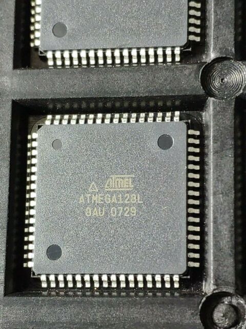
Crack Locked ATMEGA128L AVR Chip and readout atmega128l microcontroller flash memory firmware, the secured heximal file of atmega128l mcu can be deciphered from its flash memory;
When the WDE is written to logic one, the Watchdog Timer is enabled, and if the WDE is written to logic zero, the Watchdog Timer function is disabled to break off atmega128l chipset fuse bit. WDE can only be cleared if the WDCE bit has logic level one. To disable an enabled Watchdog Timer, the following procedure must be followed:
- In the same operation, write a logic one to WDCE and WDE. A logic one must be written to WDE even though it is set to one before the disable operation starts
- Within the next four clock cycles, write a logic 0 to This disables the Watchdog
- Bits .0 – WDP2, WDP1, WDP0: Watchdog Timer Prescaler 2, 1, and 0
The WDP2, WDP1, and WDP0 bits determine the Watchdog Timer prescaling when the Watch- dog Timer is enabled. The different prescaling values and their corresponding Timeout Periods are shown in Table 17.
rompa el chip ATMEGA128L avr bloqueado y lea el firmware de la memoria flash del microcontrolador atmega128l, el archivo heximal seguro de atmega128l mcu se puede descifrar desde su memoria flash
The following code example shows one assembly and one C function for turning off the WDT. The example assumes that interrupts are controlled (for example, by disabling interrupts glob- ally) so that no interrupts will occur during execution of these functions.
attack avr mcu atmega128l protection and dump binary program from atmega128l flash memory
In this mode, the Watchdog Timer is initially disabled, but can be enabled by writing the WDE bit to 1 without any restriction. A timed sequence is needed when changing the Watchdog Time-out period or disabling an enabled Watchdog Timer by breaking atmega128l microcontroller flash memory. To disable an enabled Watchdog Timer and/or changing the Watchdog Time-out, the following procedure must be followed:
- In the same operation, write a logic one to WDCE and WDE. A logic one must be written to WDE regardless of the previous value of the WDE bit
- Within the next four clock cycles, in the same operation, write the WDE and WDP bits as desired, but with the WDCE bit cleared
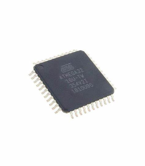
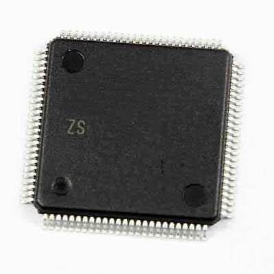
ATMEL AVR Microcontroller ATmega32 Flash Memory Breaking
ATMEL AVR Microcontroller ATmega32 Flash Memory Breaking is a process to clone embedded code from atmega32 mcu flash memory, the firmware of flash memory of avr mcu atmega32 can be readout;
ATMEL AVR Microcontroller ATmega32 Flash Memory Breaking is a process to clone embedded code from atmega32 mcu flash memory, the firmware of flash memory of avr mcu atmega32 can be readout
The Register File is optimized for the AVR Enhanced RISC instruction set. In order to achieve the required performance and flexibility, the following input/output schemes are supported by the Register File:
- One 8-bit output operand and one 8-bit result input
- Two 8-bit output operands and one 8-bit result input
- Two 8-bit output operands and one 16-bit result input
- One 16-bit output operand and one 16-bit result input
Figure 3 shows the structure of the 32 general purpose working registers in the CPU.
Most of the instructions operating on the Register File have direct access to all registers, and most of them are single cycle instructions.
ATMEL AVR microcontrolador ATmega32 romper la memoria flash es un proceso para clonar código embebido de la memoria flash mcu atmega32, el firmware de la memoria flash de avr mcu atmega32 puede ser readout;
As shown in Figure 3, each register is also assigned a Data memory address, mapping them directly into the first 32 locations of the user Data Space. Although not being physically implemented as SRAM locations, this memory organization provides great flexibility in access of the registers to copy avr microcontroller atmega32 flash software, as the X-pointer, Y-pointer, and Z-pointer Registers can be set to index any register in the file.
The registers R26..R31 have some added functions to their general purpose usage. These reg- isters are 16-bit address pointers for indirect addressing of the Data Space. The three indirect address registers X, Y and Z are defined as described in Figure 4.
The Stack is mainly used for storing temporary data, for storing local variables and for storing return addresses after interrupts and subroutine calls. The Stack Pointer Register always points to the top of the Stack. Note that the Stack is implemented as growing from higher memory loca- tions to lower memory locations. This implies that a Stack PUSH command decreases the Stack Pointer.
crack avr atmel microprocessor atmega32 fuse bit and extract embedded code from atmega32 mcu flash memory
The Stack Pointer points to the data SRAM Stack area where the Subroutine and Interrupt Stacks are located. This Stack space in the data SRAM must be defined by the program before any subroutine calls are executed or interrupts are enabled. The Stack Pointer must be set to point above 0x60 by recovering atmega32 microprocessor flash memory content.
The Stack Pointer is decremented by one when data is pushed onto the Stack with the PUSH instruction, and it is decremented by two when the return address is pushed onto the Stack with subroutine call or interrupt. The Stack Pointer is incremented by one when data is popped from the Stack with the POP instruction, and it is incremented by two when address is popped from the Stack with return from subroutine RET or return from interrupt RETI.
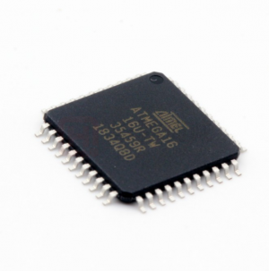
Unlock Encrypted MCU ATmega16 Heximal
Unlock Encrypted MCU ATmega16 Heximal will need engineer to attack atmega16 microcontroller protection system then readout embedded source code from atmega16 microprocessor flash memory;
Unlock Encrypted MCU ATmega16 Heximal will need engineer to attack atmega16 microcontroller protection system then readout embedded source code from atmega16 microprocessor flash memory;
The EEPROM Address Registers – EEARH and EEARL – specify the EEPROM address in the 512bytes EEPROM space. The EEPROM data bytes are addressed linearly between 0 and 511. The initial value of EEAR is undefined. A proper value must be written before the EEPROM may be accessed.
For the EEPROM write operation, the EEDR Register contains the data to be written to the EEPROM in the address given by the EEAR Register. For the EEPROM read operation, the EEDR contains the data read out from the EEPROM at the address given by EEAR.
desbloquear cifrado MCU ATmega16 heximal necesitará ingeniero para atacar atmega16 microcontrolador sistema de protección a continuación, leer código fuente embebido de atmega16 microprocesador de memoria flash
The EEMWE bit determines whether setting EEWE to one causes the EEPROM to be written. When EEMWE is set, setting EEWE within four clock cycles will write data to the EEPROM at the selected address If EEMWE is zero to copying atmega165 mcu firmware, setting EEWE will have no effect. When EEMWE has been written to one by software, hardware clears the bit to zero after four clock cycles.
Unlock Encrypted MCU ATmega16 Heximal will need engineer to attack atmega16 microcontroller protection system then readout embedded source code from atmega16 microprocessor flash memory
The EEPROM Write Enable Signal EEWE is the write strobe to the EEPROM. When address and data are correctly set up, the EEWE bit must be written to one to write the value into the EEPROM. The EEMWE bit must be written to one before a logical one is written to EEWE, otherwise no EEPROM write takes place. The following procedure should be followed when writing the EEPROM (the order of steps 3 and 4 is not essential):
- Wait until EEWE becomes zero
- Wait until SPMEN in SPMCR becomes zero
- Write new EEPROM address to EEAR (optional)
- Write new EEPROM data to EEDR (optional)
- Write a logical one to the EEMWE bit while writing a zero to EEWE in EECR
Within four clock cycles after setting EEMWE, write a logical one to EEWE by breaking atmega16 microcontroller fuse bit;
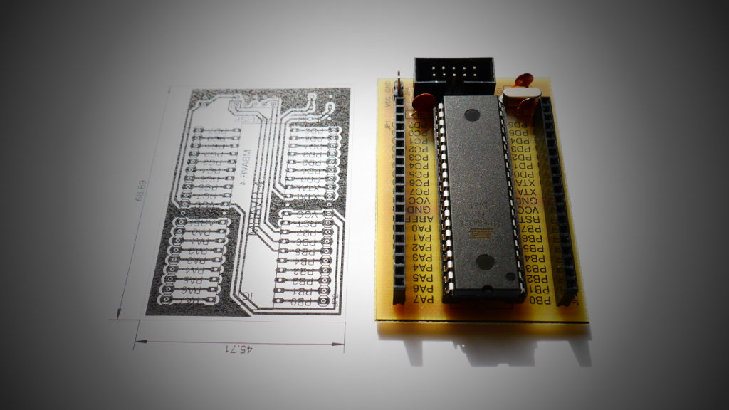
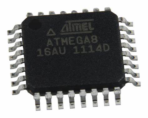
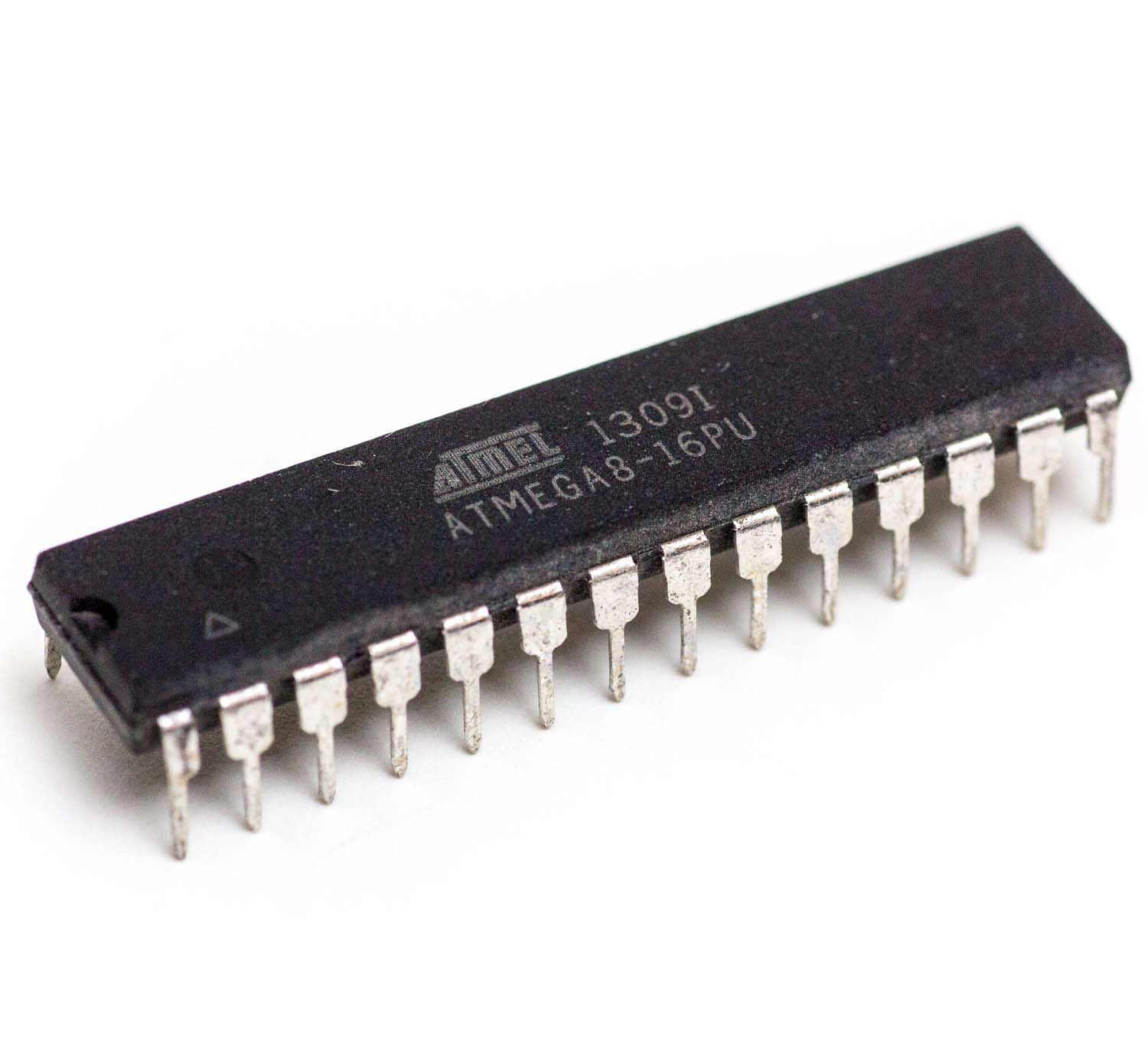
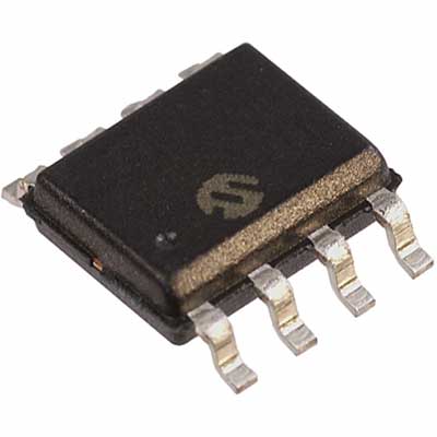
Break ATmega8 Encrypted MCU Fuse Bit
Break ATmega8 Encrypted MCU Fuse Bit by focus ion beam will help engineer to copy avr chip atmega8 microcontroller flash firmware, after extract embedded firmware from microprocessor atmega8 secured flash memory;
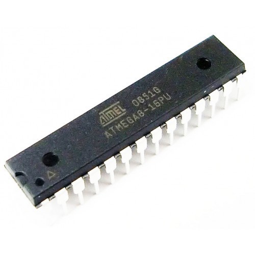
Break ATmega8 Encrypted MCU Fuse Bit by focus ion beam will help engineer to copy avr chip atmega8 microcontroller flash firmware, after extract embedded firmware from microprocessor atmega8 secured flash memory
The boot program can use any interface to download the application program in the Application Flash memory. Software in the Boot Flash Section will continue to run while the Application Flash Section is updated, providing true Read-While-Write operation by recovery atmega8 mcu flash memory content. By combining an 8-bit RISC CPU with In-System Self-Programmable Flash on a monolithic chip, the Atmel ATmega8 is a powerful microcontroller that provides a highly-flexible and cost-effective solution to many embedded control applications.
Leer AVR ATMEGA8L Microcontrolador Código Protegido necesita ingeniería inversa atmega8l mcu sistema de resistencia a la manipulación y, a continuación, recuperar el firmware embebido de atmega8l microprocesador de memoria flash;
The ATmega8 is supported with a full suite of program and system development tools, including C compilers, macro assemblers, program simulators, and evaluation kits.
secured atmega8 mcu protection cracking can recover heximal from microcontroller atmega8 flash memory
Typical values contained in this datasheet are based on simulations and characterization of other AVR microcontrollers manufactured on the same process technology. Minimum and Maxi- mum values will be available after the device is characterized.
Port B is an 8-bit bi-directional I/O port with internal pull-up resistors (selected for each bit). The Port B output buffers have symmetrical drive characteristics with both high sink and source capability. As inputs, Port B pins that are externally pulled low will source current if the pull-up resistors are activated. The Port B pins are tri-stated when a reset condition becomes active, even if the clock is not running.
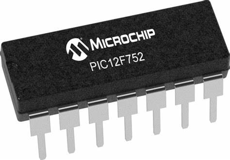
Break Microchip PIC12F752 Locked MCU Flash Memory
Break Microchip PIC12F752 Locked MCU Flash Memory protection over its fuse bit and readout embedded heximal program from PIC12F752 Microcontroller for cloning;
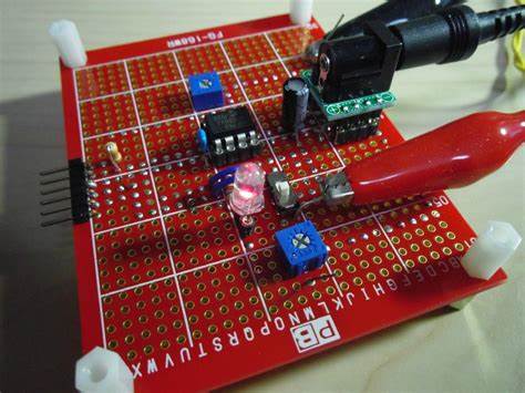
Break Microchip PIC12F752 Locked MCU Flash Memory protection over its fuse bit and readout embedded heximal program from PIC12F752 Microcontroller for cloning;
For oscillator modes involving a crystal or resonator (HS, HSPLL, LP or XT), the situation is somewhat dif- ferent. Since the oscillator may require a start-up time considerably longer than the FCSM sample clock time, a false clock failure may be detected.
romper microchip PIC12F752 bloqueado MCU protección de memoria flash sobre su bit de fusible y la lectura incrustado programa heximal de PIC12F752 Microcontrolador para la clonación;
To prevent this, the internal oscillator block is automatically configured as the system clock and functions until the primary clock is stable (the OST and PLL timers have timed out) to readout pic12f509 flash memory file. This is identical to Two-Speed Start-up mode. Once the primary clock is stable, the INTRC returns to its role as the FSCM source.
Recover embedded binary file from Microprocessor PIC12F752 flash memory
As noted in Section 19.3.1 “Special Considerations for Using Two-Speed Start-up”, it is also possible to select another clock configuration and enter an alter- nate power managed mode while waiting for the primary system clock to become stable. When the new powered managed mode is selected, the primary clock is disabled.
The same logic that prevents false oscilla- tor failure interrupts on POR or wake from Sleep will also prevent the detection of the oscillator’s failure to start at all following these events. This can be avoided by monitoring the OSTS bit and using a timing routine to determine if the oscillator is taking too long to start. Even so, no oscillator failure interrupt will be flagged.
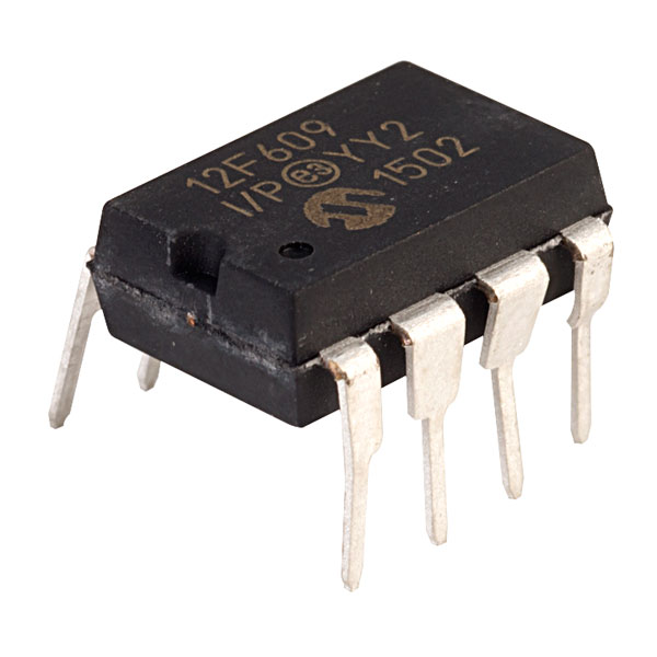
Unlock Microchip PIC12F609 Processor Flash Content
Unlock Microchip PIC12F609 Processor Flash Content and extract heximal file to new Microcontroller pic12f609;
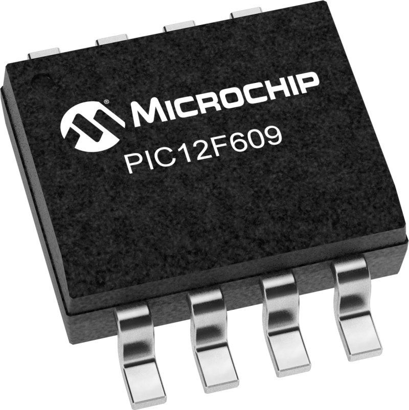
Desbloquee el contenido flash del procesador Microchip PIC12F609 y extraiga el archivo heximal al nuevo microcontrolador pic12f609;
This would allow an application to briefly wake-up, perform routine “housekeeping” tasks and return to Sleep before the device starts to operate from the primary oscillator.
User code can also check if the primary clock source is currently providing the system clocking by checking the status of the OSTS bit (OSCCON<3>). If the bit is set, the primary oscillator is providing the system clock. Otherwise, the internal oscillator block is providing the clock during wake-up from Reset or Sleep mode.
The Fail-Safe Clock Monitor (FSCM) allows the micro- controller to continue operation, in the event of an external oscillator failure, by automatically switching the system clock to the internal oscillator block by extracting pic12f617 microcontroller source code. The FSCM function is enabled by setting the Fail-Safe Clock Monitor Enable bit, FSCM (CONFIG1H<6>).
Odblokuj zawartość Flash procesora Microchip PIC12F609 i wyodrębnij plik szesnastkowy do nowego mikrokontrolera pic12f609
When FSCM is enabled, the INTRC oscillator runs at all times to monitor clocks to peripherals and provide an instant backup clock in the event of a clock failure. Clock monitoring (shown in Figure 19-3) is accom- plished by creating a sample clock signal, which is the INTRC output divided by 64 when breaking off the protection over pic16f627 mcu fuse bit. This allows ample time between FSCM sample clocks for a peripheral clock edge to occur. The peripheral system clock and the sample clock are presented as inputs to the Clock Monitor latch (CM). The CM is set on the falling edge of the system clock source, but cleared on the rising edge of the sample clock.
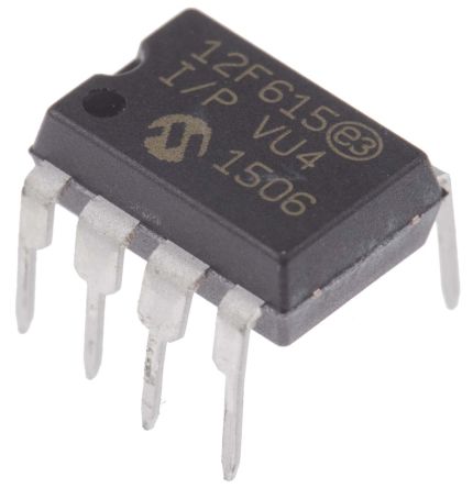
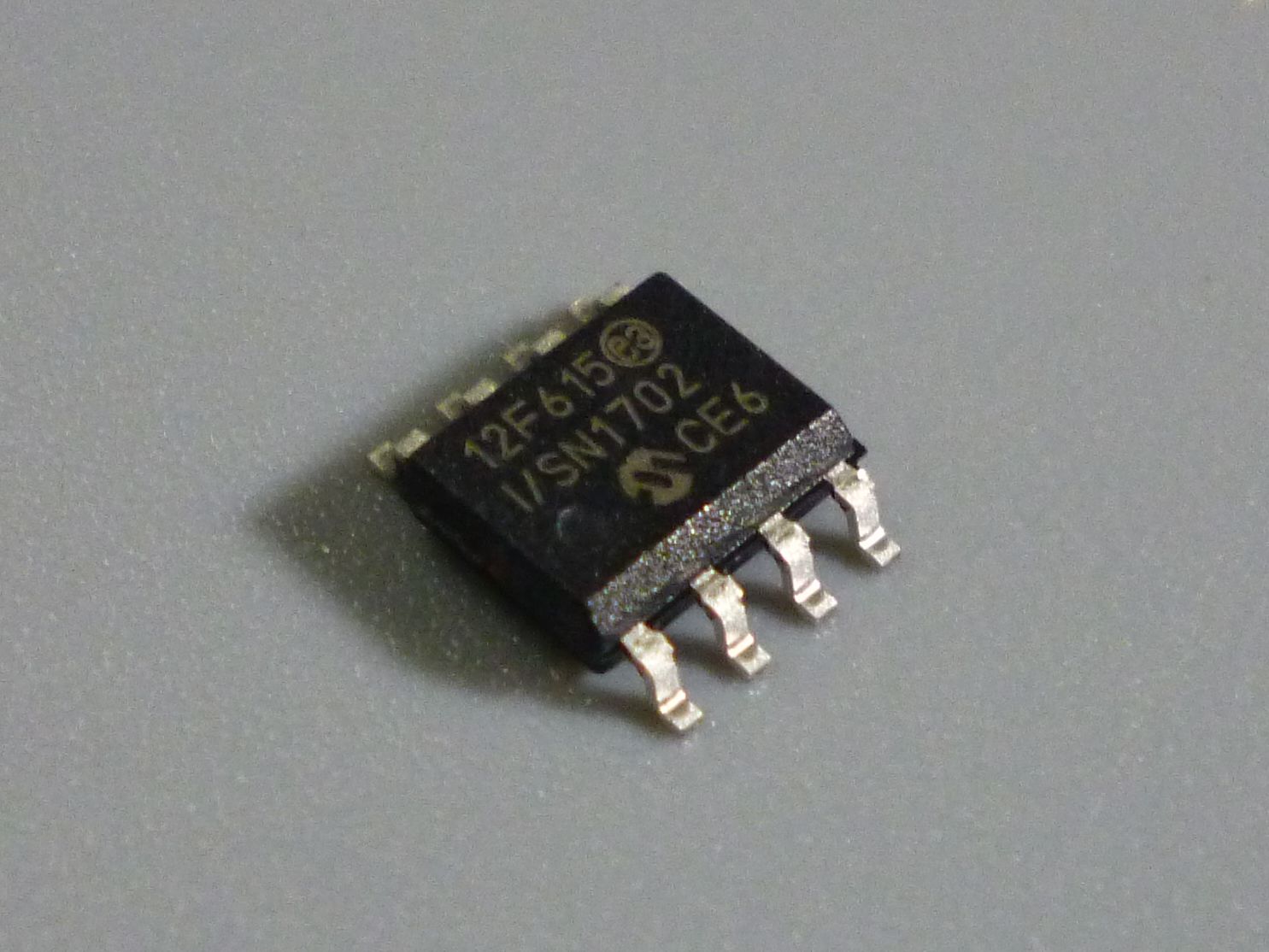
Unlock Microchip PIC12F615 MCU Flash Memory
Unlock Microchip PIC12F615 MCU Flash Memory and extract embedded firmware from PIC12F615 microcontroller original IC MCU PIC12F615 chip protection can be broken off;
Entsperren Sie den Microchip PIC12F615 MCU-Flash-Speicher und extrahieren Sie die eingebettete Firmware aus dem PIC12F615-Mikrocontroller. Der ursprüngliche IC-MCU-PIC12F615-Chipschutz kann abgebrochen werden.
For PIC12F615 devices, the WDT is driven by the INTRC source. When the WDT is enabled, the clock source is also enabled. The nominal WDT period is 4 ms and has the same stability as the INTRC oscillator to break microchip pic12f1571 mcu protection.
The 4 ms period of the WDT is multiplied by a 16-bit postscaler. Any output of the WDT postscaler is selected by a multiplexer, controlled by bits in Configuration Register 2H. Available periods range from 4 ms to
131.072 seconds (2.18 minutes). The WDT and postscaler are cleared when any of the following events occur: execute a SLEEP or CLRWDT instruction by breaking microchip pic12f508 processor flash memory, the IRCF bits (OSCCON<6:4>) are changed or a clock failure has occurred.
Entsperren Sie den Microchip PIC12F615 MCU-Flash-Speicher und extrahieren Sie die eingebettete Firmware aus dem PIC12F615-Mikrocontroller. Der ursprüngliche IC-MCU-PIC12F615-Chipschutz kann abgebrochen werden.
Adjustments to the internal oscillator clock period using the OSCTUNE register also affect the period of the WDT by the same factor. For example, if the INTRC period is increased by 3%, then the WDT period is increased by 3%.
Register 19-14 shows the WDTCON register. This is a readable and writable register, which contains a control bit that allows software to override the WDT enable Configuration bit, only if the Configuration bit has disabled the WDT.
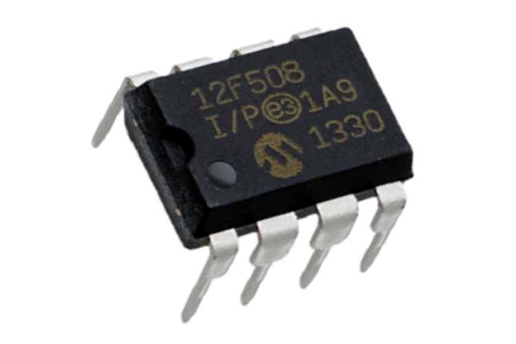
Microchip PIC12F508 Processor Flash Memory Breaking
Microchip PIC12F508 Processor Flash Memory Breaking will disable the protection over the flash memory, original embedded firmware will be read through programmer;
Przerwanie pamięci flash procesora Microchip PIC12F508 spowoduje wyłączenie ochrony pamięci flash, oryginalne wbudowane oprogramowanie sprzętowe zostanie odczytane przez programator
If the low-power mode clock frequency is less than 1 MHz, the A/D RC clock source should be selected. Operation in the Low-Power Sleep mode requires the A/ D RC clock to be selected. If bits, ACQT2:ACQT0, are set to ‘000’ and a conversion is started, the conversion will be delayed one instruction cycle to allow execution of the SLEEP instruction and entry to Low-Power Sleep mode by recovering pic12f508 mcu source code. The IDLEN and SCS bits in the OSCCON register must have already been cleared prior to starting the conversion.
The ADCON1, TRISA and TRISB registers all configure the A/D port pins. The port pins needed as analog inputs must have their corresponding TRIS bits set (input). If the TRIS bit is cleared (output), the digital output level (VOH or VOL) will be converted. The A/D operation is independent of the state of the CHS2:CHS0 bits and the TRIS bits.
Mikrokontroler Microchip PIC12F508 łamie i wyodrębnia plik szesnastkowy z jego pamięci flash i pamięci eeprom,
When reading the Port register, all pins configured as analog input channels will read as cleared (a low level). Pins con- figured as digital inputs will convert an analog input. Analog levels on a digitally configured input will be accurately converted to decrypt locked chip pic12f508 firmware from its flash memory.
Analog levels on any pin defined as a digital input may cause the digital input buffer to consume current out of the device’s specification limits.
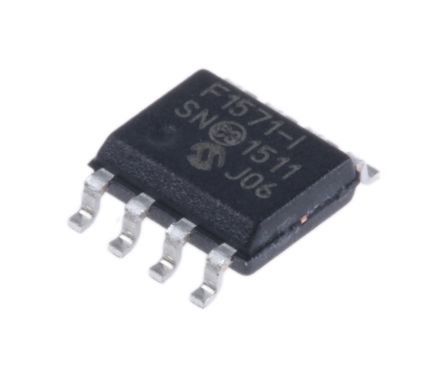
Break Microchip PIC12F1571 MCU Protection
Break Microchip PIC12F1571 MCU Protection and read embedded firmware out from pic12f1571 microcontroller flash and eeprom memory, and then clone heximal program to new microprocessor PIC12F1571;
Break Microchip PIC12F1571 MCU Protection and read embedded firmware out from pic12f1571 microcontroller flash and eeprom memory, and then clone heximal program to new microprocessor PIC12F1571
PIC12F1257 microcontrollers combine the capabilities of 16-bit PWMs with Analog to suit a variety of applications. These devices deliver four 16-bit PWMs with independent timers for applications where high resolution is needed, such as LED lighting, stepper motors, power supplies and other general purpose applications which is useful.
The core independent peripherals (16-bit PWMs, Complementary Waveform Generator), Enhanced Universal Synchronous Asynchronous Receiver Transceiver (EUSART) and Analog (ADCs, Comparator and DAC) enable closed-loop feedback and communication for use in multiple market segments to restoring pic16f870 mcu heximal code.
The Peripheral Pin Select (PPS) functionality allows for I/O pin remapping of the digital peripherals for increased flexibility. The EUSART peripheral enables the communication for applications such as LIN.
Сломайте защиту микроконтроллера Microchip PIC12F1571 и прочитайте встроенную прошивку из флэш-памяти микроконтроллера pic12f1571 и памяти eeprom, а затем клонируйте шестнадцатеричную программу в новый микропроцессор PIC12F1571.
For the A/D converter to meet its specified accuracy, the charge holding capacitor (CHOLD) must be allowed to fully charge to the input channel voltage level. The analog input model is shown in Figure 17-2. The source impedance (RS) and the internal sampling switch (RSS) impedance directly affect the time required to charge the capacitor CHOLD by extracting mcu pic18f2520 embedded firmware.
The sampling switch (RSS) impedance varies over the device voltage (VDD). The source impedance affects the offset voltage at the analog input (due to pin leakage current). The maximum recommended impedance for analog sources is 2.5 kW. After the analog input channel is selected (changed), the channel must be sampled for at least the minimum acquisition time before starting a conversion.
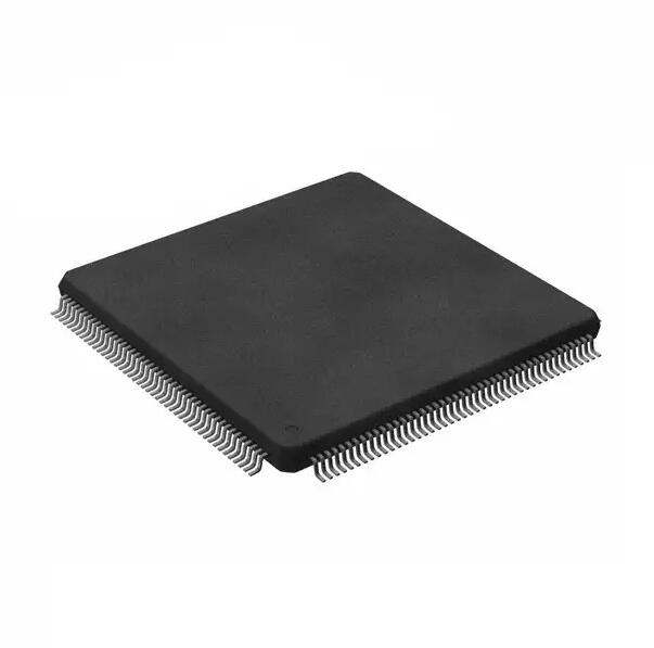
Break DSP TMS320F2810PBKS Microcontroller Locked Memory
Break DSP TMS320F2810PBKS Microcontroller Locked Memory and extract mcu tms320f2810pb flash memory content, original embedded firmware will be restored from microprocessor tms320f2810pb dsp mcu;
The 2803x devices incorporate a method to reduce the device current consumption. Because each peripheral unit has an individual clock-enable bit, significant reduction in current consumption can be achieved by turning off the clock to any peripheral module that is not used in a given application.
romper DSP TMS320F2810PBKS microcontrolador bloqueado la memoria y extraer mcu tms320f2810pb contenido de la memoria flash, el firmware original incrustado será restaurado desde el microprocesador tms320f2810pb dsp mcu
Furthermore, any one of the three low-power modes could be taken advantage of to reduce the current consumption even further to attack ic mcu tms320f28232pg software. Below Table indicates the typical reduction in current consumption achieved by turning off the clocks.
All peripheral clocks (except CPU Timer clock) are disabled upon reset. Writing to/reading from peripheral registers is possible only after the peripheral clocks are turned on.
This number represents the current drawn by the digital portion of the ADC module to recover microcontroller tms320f2812pg firmware. Turning off the clock to the ADC module results in the elimination of the current drawn by the analog portion of the ADC (IDDA) as well.
For peripherals with multiple instances, the current quoted is per module. For example, the 2 mA value quoted for ePWM is for one ePWM module.