Archive for April, 2019
 Recover MCU Layout Design Infringement
Recover MCU Layout Design without the consent of the right holder constitutes an infringement. There are two main types of microcontroller copying here, one is full replication, the other is partial replication.
The illegal copying of other people’s mcu layout designs will infringe on the continuous development of the integrated circuit industry and thus harm the public’s interests. A semiconductor manufacturer may have to spend millions of dollars to develop semiconductor chips, but a pirate company may need to spend hundreds of thousands of dollars to clone IC, so the pirate company can sell it at a lower price. Such chips have caused huge losses to manufacturers who develop chips.
Recover MCU Layout Design Infringement
This kind of illegal competition is extremely harmful to the sustainable development of the semiconductor industry. Therefore, it is necessary to crack down on this behavior, but the premise is that it can correctly identify such plagiarism and copying behavior in practice.
PLD Chip Reverse Engineering
In the case that property holder and defendant are competitors in the semiconductor industry. The property holder produced a PLD (Programmable Logic Device) chip to perform various logic functions. defendant produces different types of chips, called ASIC (Application-Specific Integrated Circuit), which performs different functions than the property holder’s chip. However, the property holder believes that the layout design of the chip ASIC produced by the defendant (called the mask work in the United States) duplicated layout design that he registered which is obtained from PLD Chip Reverse Engineering.
PLD Chip Reverse Engineering
PLD Chip Reverse Engineering clause on the one hand protects the interests of the owner of the layout design and on the other hand promotes technological innovation. In PLD reverse engineering, the second layout design must not be substantially the same as the first layout design.
As long as there is evidence that substantial investment and effort has been made in the development of the update new layout design, not just 100% cloning, it does not constitute infringement, even if the two layout designs are similar in some substantive parts.
The law actually allows competitors to copy microcontroller layout designs, but only if the purpose of reproduction is to develop their own original layout design.
As long as a PLD layout design embodies a low degree of creativity in any aspect, it can be considered original, and the requirements for creativity here are quite low.
In the Microcontroller reverse engineering process, competitors can take pictures and copy the registered layout design, but if competitors use this information to produce a substantially identical layout design, then it cannot be called legal reverse engineering. 1 Legal reverse engineering refers to taking pictures and copying layout designs, but the purpose of photographing and copying is to analyze the research, and combine the results of analysis and research into their own layout design to generate unique and genuine Layout design.
Breaking Original IC Layout Design
A prerequisite for the establishment of Breaking Original IC Layout Design defense is that the new layout design must be original compared to the prior layout design, and judging whether it is original or not is largely based on facts.
Breaking Original IC Layout Design
The court also held that if the replica of the IC layout design did have the intention of reverse engineering at first, but ultimately failed, then the law could not exempt his tort liability.
The written clues can prove to some extent that the layout design owner has independently created, but can not completely determine the originality of the layout design, and can not completely determine that the layout design is not acquired from Cloning IC layout design;
The Court of Appeals suggested that AMD did not use other alternative transistor configurations, but instead used the configuration of Brooktree, so it can be inferred that when infringer Breaking Original IC Layout Design of the owner chip, it did not design the layout itself, but just copied owner’s layout, so there is no way to assume that infringer is doing reverse engineering microcontroller. The court finally ruled that the defense of infringer reverse engineering is not established, and infringer constitutes infringement.
Reverse Engineering Microcontroller Layout Design
Infringer further argued that Reverse Engineering Microcontroller Layout Design on the core unit of the copyright holder layout design. It proposes that, according to the law, if the microcontroller layout design is developed through reverse engineering, then it is not necessary to bear the tort liability.
Reverse Engineering Microcontroller Layout Design
In the instructions given to the jury, the court pointed out that if the non-rights person reverse engineered and studied the layout design of others’ microcontroller, analyzed the circuit structure, and then integrated the analysis results into his own layout design, it did not constitute infringement.
The instructions emphasize that if infringer’s layout design contains its own new design elements, an improvement or an alternative to the copyright holder layout design, then the layout design is original.
It also explains that the layout design obtained through reverse engineering can be considered as original and therefore does not constitute infringement, but only if it is not substantially similar to the protected layout design, and its design contains significant Hard work and commitment, not just copying.
The instructions also remind the jury to focus on whether the defendant’s layout design is an original microcontroller layout design obtained through reverse engineering.
Infringer pointed out that it has made a lot of investment in the process of developing microcontroller layout design, and the Semiconductor Chip Protection Act prohibits the investment of very small plagiarism, rather than the reverse engineering behavior that has invested a lot of time and energy.
It also presented a paper trail to prove that it was a mcu reverse engineering rather than a simple microcontroller copy. Infringer has always stressed that he has no intention of copying copyright holder’s layout design, and he has not done so. As can be seen from the written traces, Infringer spent more than $3 million and two and a half years to analyze copyright holder’s layout design.
Infringer points out that if you want to copy copyright holder’s layout design, it only takes a few months, not a few years. At the same time, Infringer proposed that its controlled semiconductor chip is smaller and faster than copyright holder’s chip.
MCU Reverse Engineering Process
In the development of the integrated circuit industry, MCU reverse engineering plays a huge role in promoting the faster design of MCU products with the same basic functions but better performance, smaller size and lower cost.
Integrated circuit technology is one of the fastest growing and most dynamic technologies in the world. With the continuous improvement of the performance of integrated circuits, the functions are continuously enhanced, and the application surface is expanding. The integrated circuit industry has become a pillar industry of the national economy and has become a driving force. One of the main factors in the world of today’s information society.
MCU Reverse Engineering Process
Experience has shown that it takes three years or longer time to completely develop a new microcontroller independently, and it takes one years or more to redesign MCU from the circuitry pattern which has been obtained from MCU reverse engineering process;
If it is MCU copied directly, It only takes three to five months. It can be seen that the application of MCU source code reverse engineering to develop Microcontrollers still requires considerable investment, so it does not deviate from the principle of fair competition.
It is precisely because of MCU reverse engineering:
1st of all, the basic principles of this technique isn’t excessively violate the fair competition. Secondly, the development of the integrated circuit industry will be vigorously promoted. Therefore, countries generally recognize MCU reverse engineering in the legislation of integrated circuits.
However, the reverse engineering is to crack MCU‘s key technology of others’ design. On the basis of this, the layout design obtained will inevitably contain the imitation and copying of the prior microcontroller layout design, so it is easy to generate infringement disputes. In the event of an infringement dispute, the accused infringer must be defended on the grounds of reverse engineering, and a series of more complicated problems will be highlighted.
Microcontroller Reverse Engineering Behavior
In the development of the Integrated circuit industry, Microcontroller Reverse Engineering behavior is common. This behavior is beneficial to designing integrated circuit products with the same basic functions but better performance, smaller size and lower cost.
The technological advancement of the integrated circuit industry does not unduly violate the principle of fair competition. Therefore, countries generally recognize the legitimacy of microcontroller reverse engineering behavior in the Integrated circuit protection law, which makes reverse engineering IC an important defense tools for integrated circuit copyright infringement.
Microcontroller Reverse Engineering Behavior
However, reverse engineering is method to dissipate and acquire the key technology of other designer (property owner). On the basis of this, the layout design obtained will inevitably contain the imitation and microcontroller copying of the prior layout design, so it is easy to be confused with the infringement, thus causing disputes.
Therefore, it is very necessary to make an accurate distinction between infringement and reverse engineering behavior. On the one hand, it helps to protect the legal rights of the owner of the layout design, avoids the infringer’s use of reverse engineering IC as a defense tool to escape legal sanctions, and on the other hand enables the person implementing reverse engineering to correctly assess the legal risk of his behavior. To understand whether it is possible to suspect infringement litigation and how to circumvent it, so that the integrated circuit industry will develop in a healthy and orderly direction.
On the basis of introducing the basic knowledge of integrated circuit, circuitry layout design and MCU reverse engineering, the article focuses on the judgment standard of integrated circuit infringement and the judgment standard of microcontroller reverse engineering behavior, thus clarifying the relationship between infringement and reverse engineering behavior.
Microcontroller with Wide Data Bus Memory Content Extraction
The microprobing experiments showed how easily a Microcontroller with Wide Data Bus Memory Content Extraction can accomplished. The fact that only a single bit in the instruction set could defeat branch instructions could pose some security implications. Also, the presence of a weak pull-up in the data bus results in the cut bus lines to stuck at logic.
Microcontroller with Wide Data Bus Memory Content Extraction
However, if a memory encryption was used this would require more sophisticated approach, for example, by injecting random data and observing the response from the CPU [12]. Nevertheless, high orthogonality of instruction sets in most RISC CPUs could help the attacker in finding the right combination to influence the MCU code execution.
Live Microcontroller decapsulation experiments proved the possibility of opening up battery powered devices without interrupting their constant power supply. This might have some consequences for highly secure applications where such devices are used. This could be medical devices or hardware security modules (HSM) used in banking or industrial applications.
Once the surface of the chip with battery-backed SRAM is accessed, the contents of the memory could be microprobed either by microprobing exposed data bus lines [12] or by exploiting test points. Both approaches though would require the use of a laser cutter to cut through passivation layer [2]. For devices fabricated with deep submicron process a Focused Ion Beam (FIB) machine will be required to establish a connection with internal data bus. However, such machines are available in many places for rent at a price below $100 per hour.
Decapsulate Microcontroller Silicon Package
Decapsulate Microcontroller Silicon Package which has helped to provide the protection over the chip wafer from moisture and air, microcontroller can be decapsulated using 100% Nitric acid heated to 60°C. It was added in small drops and washed away with acetone after a few seconds.
Decapsulate Microcontroller Silicon Package
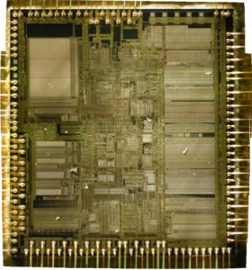
This MCU decapsulation process was repeated for several minutes until the surface of the chip die was exposed. Although the bonding wires were also exposed, this did not create any short circuits because of the high concentration of the acid. Once the IC decapsulation was finished, the whole sample was cleaned in acetone using ultrasonic bath. That removed the remaining of the acid and particles of resin. As a result the surface of the chip became clean. After careful removal of the tapes and testing the device demonstrated full functionality (below Figure).
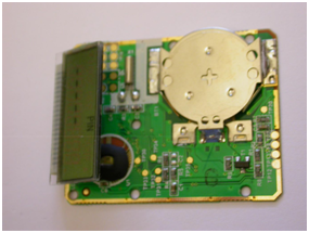
PCB of the security token after live decapsulation
It is very important to make sure that the microcontroller is not over-decapsulated. This would result in the acid going into contact with PCB traces made of copper. They react very actively with acid and this will quickly result in loss contact with bonding wires. The device with live battery connection could then be used for further IC extraction of the embedded SRAM using microprobing MCU attacks.
Microcontroller Content Sensitive to External Power Supply Recovery
Microcontroller Content Sensitive to External Power Supply Recovery has long been viewed as impossible to crack MCU with battery powered embedded SRAM was chosen – Vasco Digipass 270 – two-factor authentication token [11]. Although such devices do not have very high level of security protection like devices with tamper resistant enclosure, they offer adequate level of protection against all sorts of MCU attacks. The reason for that is because the embedded SRAM is sensitive to the fluctuations of external power supply. Any interruption of the supply will cause the loss of data. In this case the signing key. Moreover, even the hardware reset of the device will make it inoperable, resulting in all keys and the user PIN being wiped off.
Microcontroller Content Sensitive to External Power Supply Recovery
The device is relatively easy to disassemble as the internal electronics is only covered with plastic sheets glued to its plastic case. The main component of the device is a specialised microcontroller which is bonded directly to the PCB and encapsulated with epoxy. Removing the battery for more than a few seconds results in the device going into internal test mode and no longer operational.
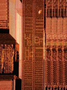
The same happens if the Reset line of the microcontroller is shorted to 0. The result of the successful partial decapsulation of the microcontroller is shown in below Figure. However, because the battery was removed for that process, the microcontroller had no useful information inside.
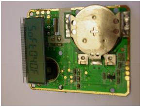
PCB of the security token after normal decapsulation
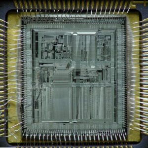
In order to verify the idea of live decapsulation, the PCB of the fully working token was first wrapped in an insulation tape, while the potted chip was covered with aluminium tape (below Figure). Then the whole setup was wrapped into aluminium tape before creating a cut in the tape where the decapsulation was desired.
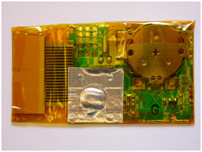
PCB of the security token prepared for live decapsulation
Secure Microcontroller Memory Recovery
As a first target to demonstrate the affordable process of Secure Microcontroller Memory Recovery, an early 2000s smartcard was chosen. It is based on the Hitachi HD6483102 chip fabricated with 0.8μm process with 2 metal layers and has embedded Mask ROM and EEPROM.
Secure Microcontroller Memory Recovery
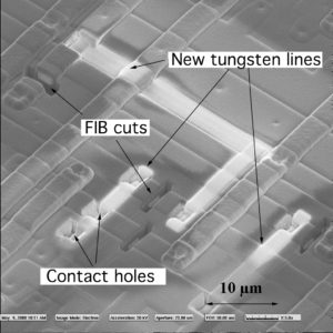
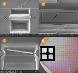
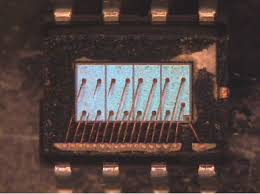
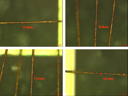
The Mask ROM is protected against optical MCU reading with doping encoding. The Von-Newmann RISC 16-bit CPU with H8/300 architecture of this chip allows access to all resources in the linear address space and has a relatively simple instruction set [10]. The interesting property of this instruction set is if the most significant bit equals to 1 then the CPU will always execute single-cycle instructions without any branches. This can be achieved with a laser cutter [2] and the result is shown in Fig. 3.
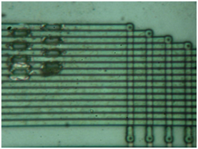
Figure 3 Cuts in the data bus lines to modify instructions
In order to microprobe the data bus only opening in the passivation layer is required (Fig. 4). This cavity will help in holding the tip of the needle in place during the microprobing process.
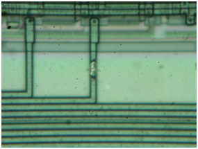
Figure 4 Opening in passivation layer above the data bus line
Once the CPU is forced into execution of simple instructions it will access the whole memory by fetching all the addresses sequentially. This way the memory contents can be extracted by placing a microprobing needle over each bit of the data bus one at a time and recording the information on a digital storage oscilloscope. After that all the acquisitions could be synchronised with the Reset signal.