Archive for October, 2018
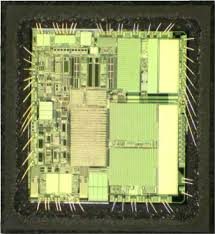
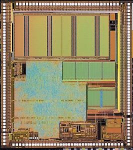
 PIC18F4523 Microcontroller Embedded Memory Breaking
Many PIC18 control instructions do not need any argument at all by Break IC STM32F101C4T6TR Binary; they either perform an operation that globally affects the device or they operate implicitly on one register after PIC18F4523 Microcontroller Embedded Memory Breaking. This addressing mode is known as Inherent Addressing. Examples include SLEEP, RESET and DAW.
Other instructions work in a similar way but require an additional explicit argument in the opcode to Break Chip SAF-C164CI-8EM Firmware. This is known as Literal Addressing mode because they require some literal value as an argument. Examples include ADDLW and MOVLW, which respectively, add or move a literal value to the W register. Other examples include CALL and GOTO, which include a 20-bit program memory address.
Direct Addressing mode specifies all or part of the source and/or destination address of the operation within the opcode itself. The options are specified by the arguments accompanying the instruction.
PIC18F4523 Microcontroller Embedded Memory Breaking
In the core PIC18 instruction set, bit-oriented and byte- oriented instructions use some version of Direct Addressing by default to better support Break Microcontroller PIC12F629 Program. All of these instructions include some 8-bit literal address as their Least Significant Byte when PIC18F4523 Microcontroller Embedded Memory Breaking. This address specifies either a register address in one of the banks of data RAM through Crack MCU memory.
The Access RAM bit ‘a’ determines how the address is interpreted. When ‘a’ is ‘1’, the contents of the BSR (Section 5.3.1 “Bank Select Register (BSR)”) are used with the address to determine the complete 12-bit address of the register. When ‘a’ is ‘0’, the address is interpreted as being a register in the Access Bank to facilitate the process of Break MCU dsPIC30F4011 Heximal. Addressing that uses the Access RAM is sometimes also known as Direct Forced Addressing mode.
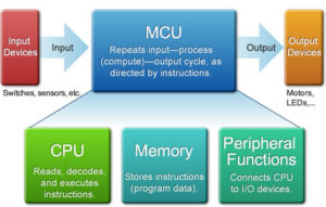
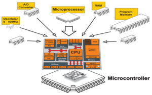
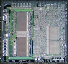
Microprocessor PIC18F4520 Program Memory Data Retrieving
The STATUS register, shown in Register 5-2, contains the arithmetic status of the ALU to provide the purpose of Microprocessor PIC18F4520 Program Memory Data Retrieving. As with any other SFR, it can be the operand for any instruction.
If the STATUS register is the destination for an instruc- tion that affects the Z, DC, C, OV or N bits, the results of the instruction are not written; instead, the STATUS register is updated according to the instruction performed by Recover MCU P89LPC925FDH Heximal. Therefore, the result of an instruction with the STATUS register as its destination may be different than intended when Crack MCU eeprom. As an example, CLRF STATUS will set the Z bit and leave the remaining Status bits unchanged (‘000u u1uu’).
Microprocessor PIC18F4520 Program Memory Data Retrieving
It is recommended that only BCF, BSF, SWAPF, MOVFF and MOVWF instructions are used to alter the STATUS register, because these instructions do not affect the Z, C, DC, OV or N bits in the STATUS register.
While the program memory can be addressed in only one way – through the program counter – information in the data memory space can be addressed in several ways and Copy Chip SAF-XC888CM-8FFI Binary is one of them. For most instructions, the addressing mode is fixed. Other instructions may use up to three modes, depending on which operands are used by Copy Microcontroller AT89C51RE2 Binary and whether or not the extended instruction set is enabled.
The addressing modes are:
- Inherent
- Literal
- Direct
- Indirect
An additional addressing mode, Indexed Literal Offset, is available when the extended instruction set is enabled (XINST Configuration bit = 1).
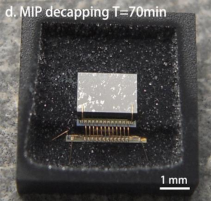
Microchip PIC18F4515 Embedded Firmware Restoration
Microchip PIC18F4515 Embedded Firmware Restoration is a process to extract the embedded heximal from PIC18F4515 after crack microcontroller PIC18F4515 protection system;
The instruction is forced to use the Access Bank address map; the current value of the BSR is ignored entirely due
to the process of Attack Microcontroller W77E058A40DL Flash. Using this “forced” addressing allows the instruction to operate on a data address in a single cycle which will facilitate Microchip PIC18F4515 Embedded Firmware Restoration, without updating the BSR first. For 8-bit addresses of 80h and above, this means that users can evaluate and operate on SFRs more efficiently.
The Access RAM below 80h is a good place for data values that the user might need to access rapidly, such as immediate computational results or common program variables by Attack MCU ATMEGA162 Flash. Access RAM also allows for faster and more code efficient context saving and switching of variables.
The mapping of the Access Bank is slightly different when the extended instruction set is enabled (XINST Configuration bit = 1). This is discussed in more detail in Section 5.5.3 “Mapping the Access Bank in Indexed Literal Offset Mode”.
Microchip PIC18F4515 Embedded Firmware Restoration
PIC18F4515 devices may have banked memory in the GPR area. This is data RAM which is available for use by all instructions. GPRs start at the bottom of Bank 0 (address 000h) and grow downwards towards the bottom of the SFR area. GPRs are not initialized by a Power-on Reset and are unchanged on all other Resets.
The Special Function Registers (SFRs) are registers used by the CPU and peripheral modules for controlling the desired operation of the device when Microchip PIC18F4515 Embedded Firmware Restoration. These registers are implemented as static RAM. SFRs start at the top of data memory (FFFh) and extend downward to occupy the top half of Bank 15 (F80h to FFFh).
The SFRs can be classified into two sets: those associated with the “core” device functionality (ALU, Resets and interrupts) and those related to the peripheral functions obtained from Copy MCU AT89C55WD Binary. The Reset and Interrupt registers are described in their respective chapters, while the ALU’s STATUS register is described later in this section.
Registers related to the operation of a peripheral feature are described in the chapter for that peripheral. The SFRs are typically distributed among the peripherals whose functions they control. Unused SFR locations are unimplemented and read as ‘0’s to Crack MCU.
Microprocessor PIC18F4510 Eeprom Memory Breaking
Microprocessor PIC18F4510 Eeprom Memory Breaking
While the use of the BSR with an embedded 8-bit address allows users to address the entire range of data memory which can facilitate Microprocessor PIC18F4510 Eeprom Memory Breaking, it also means that the user must always ensure that the correct bank is selected. Otherwise, data may be read from or written to the wrong location.
This can be disastrous if a GPR is the intended target of an operation, but an SFR is written to instead. Verifying and/or changing the BSR for each read or write to data memory can become very inefficient.
To streamline access for the most commonly used data memory locations, the data memory is configured with an Access Bank, which allows users to access a mapped block of memory without specifying a BSR. The Access Bank consists of the first 128 bytes of memory (00h-7Fh) in Bank 0 and the last 128 bytes of memory (80h-FFh) in Block 15.
Microprocessor PIC18F4510 Eeprom Memory Breaking
The lower half is known as the “Access RAM” and is composed of GPRs. This upper half is also where the device’s SFRs are mapped. These two areas are mapped contiguously in the Access Bank and can be addressed in a linear fashion by an 8-bit address.
The Access Bank is used by core PIC18F4510 instructions that include the Access RAM bit (the ‘a’ parameter in the instruction). When ‘a’ is equal to ‘1’, the instruction uses the BSR and the 8-bit address included in the opcode for the data memory address. When ‘a’ is ‘0’,
PIC18F4480 Microcontroller Memory Data Recovering
PIC18F4480 Microcontroller Memory Data Recovering
Large areas of data memory require an efficient addressing scheme to make rapid access to any address possible which can provide great benefit for PIC18F4480 Microcontroller Memory Data Recovering. Ideally, this means that an entire address does not need to be provided for each read or write operation. For PIC18 devices, this is accom- plished with a RAM banking scheme.
PIC18F4480 Microcontroller Memory Data Recovering
This divides the memory space into 16 contiguous banks of 256 bytes. Depending on the instruction, each location can be addressed directly by its full 12-bit address, or an 8-bit low-order address and a 4-bit Bank Pointer.
Most instructions in the PIC18F4480 instruction set make use of the Bank Pointer, known as the Bank Select Register (BSR). This SFR holds the 4 Most Significant bits of a location’s address; the instruction itself includes the 8 Least Significant bits.
Only the four lower bits of the BSR are implemented (BSR3:BSR0). The upper four bits are unused; they will always read ‘0’ and cannot be written to. The BSR can be loaded directly by using the MOVLB instruction.
The value of the BSR indicates the bank in data memory; the 8 bits in the instruction show the location in the bank and can be thought of as an offset from the bank’s lower boundary. The relationship between the BSR’s value and the bank division in data memory is shown in below Figure.
Since up to 16 registers may share the same low-order address, the user must always be careful to ensure that the proper bank is selected before performing a data read or write. For example, writing what should be program data to an 8-bit address of F9h while the BSR is 0Fh will end up resetting the program counter.
While any bank can be selected, only those banks that are actually implemented can be read or written to. Writes to unimplemented banks are ignored, while reads from unimplemented banks will return ‘0’s. Even so, the STATUS register will still be affected as if the operation was successful. The data memory map in Figure 5-5 indicates which banks are implemented.
Recover Microprocessor PIC18F4458 Firmware Data
Device Resets on stack overflow and stack underflow conditions are enabled by setting the STVREN bit in Configuration Register 4L. When STVREN is set, a full or underflow will set the appropriate STKFUL or STKUNF bit and then cause a device Reset when Recover Microprocessor PIC18F4458 Firmware Data.
When STVREN is cleared, a full or underflow condition will set the appropriate STKFUL or STKUNF bit but not cause a device Reset after Recover MCU PIC18F2520 Binary. The STKFUL or STKUNF bits are cleared by the user software or a Power-on Reset.
Recover Microprocessor PIC18F4458 Firmware Data
A fast register stack is provided for the STATUS, WREG and BSR registers, to provide a “fast return” option for interrupts to Crack MCU. The stack for each register is only one level deep and is neither readable nor writable after Recover IC AT89C4051 Heximal. It is loaded with the current value of the corresponding register when the processor vectors for an interrupt.
All interrupt sources will push values into the stack registers. The values in the registers are then loaded back into their associated registers if the RETFIE, FAST instruction is used to return from the interrupt after Copy Microcontroller P87C51X2BBD Binary.
If both low and high priority interrupts are enabled, the stack registers cannot be used reliably to return from low priority interrupts. If a high priority interrupt occurs while servicing a low priority interrupt, the stack register values stored by the low priority interrupt will be overwritten for the purpose of Copy MCU Atmega32A Software. In these cases, users must save the key registers in software during a low priority interrupt.
Microchip PIC18F4455 Flash Memory Software Restoration
The action of Microchip PIC18F4455 Flash Memory Software Restoration that takes place when the stack becomes full depends on the state of the STVREN (Stack Over- flow Reset Enable) Configuration bit. (Refer to Section 23.1 “Configuration Bits” for a description of the device Configuration bits.) If STVREN is set (default), the 31st push will push the (PC + 2) value onto the stack when Attack Chip Atmega8A Binary, set the STKFUL bit and reset the device. The STKFUL bit will remain set and the Stack Pointer will be set to zero.
If STVREN is cleared, the STKFUL bit will be set on the 31st push and the Stack Pointer will increment to 31. Any additional pushes will not overwrite the 31st push and STKPTR will remain at 31. When the stack has been popped enough times to unload the stack by Attack Microcontroller PIC16C63A Heximal, the next pop will return a value of zero to the PC and sets the STKUNF bit, while the Stack Pointer remains at zero. The STKUNF bit will remain set until cleared by software or until a POR occurs.
Microchip PIC18F4455 Flash Memory Software Restoration
Returning a value of zero to the PC on an underflow has the effect of vectoring the program to the Reset vector, where the stack conditions can be verified and appropriate actions can be taken to Attack MCU PIC16CE625 Program. This is not the same as a Reset, as the contents of the SFRs are not affected.
Since the Top-of-Stack is readable and writable, the ability to push values onto the stack and pull values off the stack without disturbing normal program execution is a desirable feature. The PIC18 instruction set includes two instructions, PUSH and POP, that permit the TOS to be manipulated under software control. TOSU, TOSH and TOSL can be modified to place data or a return address on the stack to Crack MCU Eeprom.
The PUSH instruction places the current PC value onto the stack. This increments the Stack Pointer and loads the current PC value onto the stack. The POP instruction discards the current TOS by decrementing the Stack Pointer when Break Microcontroller PIC18F8722 Flash. The previous value pushed onto the stack then becomes the TOS value.