Archive for March, 2015
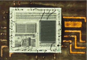
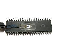
 Break IC PIC16C711 Program
We can Break IC PIC16C711 Program, please view the IC PIC16C711 features for your reference:
The clock input (from OSC1) is internally divided by four to generate four non-overlapping quadrature clocks namely Q1, Q2, Q3 and Q4. Internally, the program counter (PC) is incremented every Q1, the instruction is fetched from the program memory and latched into the instruction register in Q4.
The instruction is decoded and executed during the following Q1 through Q4. The clocks and instruction execution flow is shown in Figure 3-2. An “Instruction Cycle” consists of four Q cycles (Q1, Q2, Q3 and Q4). The instruction fetch and execute are pipelined such that fetch takes one instruction cycle while decode and execute takes another instruction cycle when Attack PIC MCU 16F506 Code.
However, due to the pipelining, each instruction effectively executes in one cycle. If an instruction causes the program counter to change (e.g.GOTO) then two cycles are required to complete the instruction (Example 3-1).
A fetch cycle begins with the program counter (PC) incrementing in Q1. In the execution cycle, the fetched instruction is latched into the “Instruction Register” (IR) in cycle Q1. This instruction is then decoded and executed during the Q2, Q3, and Q4 cycles to facilitate the progress of Recover Chip PIC16C77 Code. Data memory is break during Q2 (operand break) and written during Q4 (destination write) from Break IC PIC16C711 Program.
Circuit Engineering Company Limited continues to be recognized as the Southern China Leader in Services for IC Break, MCU Crack, Chip Extract, Microcontroller Unlock service.
Break IC PIC16C711 Program
With the advancement of today’s modern circuit board technology, it is more important than ever to have specialists available to help you at a moment’s notice. Our engineering and commercial teams collectively have a vast amount of electronic experience covering field include Consumer Electronics, Industrial Automation Electronics, Wireless Communication Electronics., etc. For more information please contact us through email.
Recover Chip PIC16C71 Code
We can Recover Chip PIC16C71 Code, please view the Chip PIC16C71 features for your reference:
The PIC16C71X is a family of low-cost, high-performance, CMOS, fully-static, 8-bit microcontrollers with integrated analog-to-digital (A/D) converters, in the PIC16CXX mid-range family.
All PIC16/17 microcontrollers employ an advanced RISC architecture. The PIC16CXX microcontroller family has enhanced core features, eight-level deep stack, and multiple internal and external interrupt sources which can be applied for Microcontroller Unlocking.
The separate instruction and data buses of the Harvard architecture allow a 14-bit wide instruction word with the separate 8-bit wide data. The two stage instruction pipeline allows all instructions to execute in a single cycle, except for program branches which require two cycles after Recover Chip PIC16C71 Code.
A total of 35 instructions (reduced instruction set) are available. Additionally, a large register set gives some of the architectural innovations used to achieve a very high performance. PIC16CXX microcontrollers typically achieve a 2:1 code compression and a 4:1 speed improvement over other 8-bit microcontrollers in their class, The PIC16C710/71 devices have 36 bytes of RAM, the PIC16C711 has 68 bytes of RAM and the PIC16C715 has 128 bytes of RAM.
Each device has 13 I/O pins. In addition a timer/counter is available. Also a 4-channel high-speed 8-bit A/D is provided which can be used for Recover IC PIC16F72A Binary. The 8-bit resolution is ideally suited for applications requiring low-cost analog interface, e.g. thermostat control, pressure sensing, etc.
Recover Chip PIC16C71 Code
The PIC16C71X family has special features to reduce external components, thus reducing cost, enhancing system reliability and reducing power consumption.
There are four oscillator options, of which the single pin RC oscillator provides a low-cost solution, the LP oscillator minimizes power consumption in order to Break Microcontroller PIC16C65B Eeprom, XT is a standard crystal, and the HS is for High Speed crystals only.
The SLEEP (power-down) feature provides a power saving mode. The user can wake up the chip from SLEEP through several external and internal interrupts and resets.
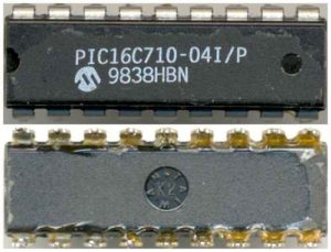
Reverse Engineering Microcontroller PIC16C710 Code
We can Reverse Engineering Microcontroller PIC16C710 Code, please view the Microcontroller PIC16C710 features for your reference:
· High-performance RISC CPU
· Only 35 single word instructions to learn
· All single cycle instructions except for program branches which are two cycle
· Operating speed: DC – 20 MHz clock input DC – 200 ns instruction cycle
· Up to 2K x 14 words of Program Memory, up to 128 x 8 bytes of Data Memory (RAM)
· Interrupt capability
· Eight level deep hardware stack
· Direct, indirect, and relative addressing modes
· Power-on Reset (POR)
· Power-up Timer (PWRT) and Oscillator Start-up Timer (OST)
· Watchdog Timer (WDT) with its own on-chip RC oscillator for reliable operation only after Attack MCU PIC16C558 Program
· Programmable code-protection
· Power saving SLEEP mode
· Selectable oscillator options
· Low-power, high-speed CMOS EPROM technology
· Fully static design
Reverse Engineering Microcontroller PIC16C710 Code
· Wide operating voltage range: 2.5V to 6.0V
· High Sink/Source Current 25/25 mA
· Commercial, Industrial and Extended temperature ranges
· Program Memory Parity Error Checking Circuitry with Parity Error Reset (PER) (PIC16C715)
· Low-power consumption:
– < 2 mA @ 5V, 4 MHz
– 15 µA typical @ 3V, 32 kHz
– < 1 µA typical standby current
Circuit Engineering Company Limited continues to be recognized as the Southern China Leader in Services for IC Read, MCU Crack, Chip Reverse engineering, Microcontroller reverse engineering service.
With the advancement of today’s modern circuit board technology, it is more important than ever to have specialists available to help you at a moment’s notice after Reverse Engineering Microcontroller PIC16C710 Code.
Our engineering and commercial teams collectively have a vast amount of electronic experience covering field include Consumer Electronics, Industrial Automation Electronics, Wireless Communication Electronics., etc. For more information please contact us through email.
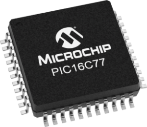
Recover Chip PIC16C77 Flash
Recover Chip PIC16C77 Flash
There are actually two 8-bit latches, one for data-out (from the PIC16/17) and one for data input. The user writes 8-bit data to PORTD data latch and Recover Chip PIC16C77 Flash. Chip Select from the port pin latch (note that they have the same address). In this mode, the TRISD register is ignored, since the microprocessor is controlling the direction of A write to the PSP occurs when both the CS and WR lines are first detected low. When either the CS or WR lines become high (level triggered), then the Input Buffer Full status flag bit IBF (TRISE<7>) is set on the Q4 clock cycle, following the next Q2 cycle, to signal the write is complete.
Recover Chip PIC16C77 Flash
The interrupt flag bit PSPIF (PIR1<7>) is also set on the same Q4 clock cycle. IBF can only be cleared by reading the PORTD input latch. The input Buffer Overflow status flag bit IBOV (TRISE<5>) is set if a second write to the Parallel Slave Port is attempted when the previous byte has not been read out of the buffer.
A read from the PSP occurs when both the CS and RD lines are first detected low. The Output Buffer Full status flag bit OBF (TRISE<6>) is cleared immediately indicating that the PORTD latch is waiting to be read by the external bus.
When either the CS or RD pin becomes high (level triggered), the interrupt flag bit PSPIF is set on the Q4 clock cycle, following the next Q2 cycle, indicating that the read is complete. OBF remains low until data is written to PORTD by the user firmware.
When not in Parallel Slave Port mode, the IBF and OBF bits are held clear. However, if flag bit IBOV was previously set, it must be cleared in firmware. An interrupt is generated and latched into flag bit PSPIF when a read or write operation is completed. PSPIF must be cleared by the user in firmware and the interrupt can be disabled by clearing the interrupt enable bit PSPIE (PIE1<7>).
The Timer0 module is a simple 8-bit overflow counter.
The clock source can be either the internal system clock (Fosc/4) or an external clock. When the clock CCP Overview source is an external clock, the Timer0 module can be selected to increment on either the rising or falling edge.
The Timer0 module also has a programmable prescaler option. This prescaler can be assigned to either the Timer0 module or the Watchdog Timer. Bit PSA (OPTION<3>) assigns the prescaler, and bits PS2:PS0 (OPTION<2:0>) determine the prescaler value.
Timer0 can increment at the following rates: 1:1 (when pres-caler assigned to Watchdog timer), 1:2, 1:4, 1:8, 1:16, 1:32, 1:64, 1:128, and 1:256 (Timer0 only). Synchronization of the external clock occurs after the prescaler. When the prescaler is used, the external clock frequency may be higher then the device’s frequency.
The maximum frequency is 50 MHz, given the high and low time requirements of the clock Timer1 is a 16-bit timer/counter. The clock source can be either the internal system clock (Fosc/4), an external clock, or an external crystal.
Timer1 can operate as either a timer or a counter. When operating as a counter (external clock source) when Recover Chip, the counter can either operate synchronized to the device or asynchronously to the device.
Asynchronous operation allows Timer1 to operate during sleep, which is useful for applications that require a real-time clock as well as the power savings of SLEEP mode. Timer1 also has a prescaler option which allows Timer1 to increment at the following rates: 1:1, 1:2, 1:4, and 1:8. Timer1 can be used in conjunction with the Capture/Compare/PWM module.
When used with a CCP module, Timer1 is the time-base for 16-bit Capture or the 16-bit Compare and must be synchronized to the device by Recover Chip PIC16C77 Flash. The CCP module(s) can operate in one of these three modes: 16-bit capture, 16-bit compare, or up to 10-bit Pulse Width Modulation (PWM).
Capture mode captures the 16-bit value of TMR1 into the CCPRxH:CCPRxL register pair. The capture event can be programmed for either the falling edge, rising edge, fourth rising edge, or the sixteenth rising edge of the CCPx pin. Compare mode compares the TMR1H:TMR1L register pair to the CCPRxH:CCPRxL register pair. When a match occurs an interrupt can be generated by Crack MCU, and the output pin CCPx can be forced to given state (High or Low), TMR1 can be reset (CCP1), or TMR1 reset and start A/D conversion (CCP2).
This depends on the control bits CCPxM3:CCPxM0. PWM mode compares the TMR2 register to a 10-bit duty cycle register (CCPRxH:CCPRxL<5:4>).
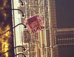
Reverse Engineering Microcontroller PIC16C76 Heximal
Reverse Engineering Microcontroller PIC16C76 Heximal
Any instruction which writes, operates internally as a read followed by a write operation. The BCF and BSF instructions, for example, read the register into the CPU, execute the bit operation and write the result back to the register. Caution must be used when these instructions are applied to a port with both inputs and outputs defined after Reverse engineeringMicrocontroller.
For example, a BSF operation on bit5 of PORTB will cause all eight bits of PORTB to be read into the CPU. Then the BSF operation takes place on bit5 and PORTB is written to the output latches.
If another bit of PORTB is used as a bi-directional I/O pin (e.g., bit0) and it is defined as an input at this time, the input signal present on the pin itself would be read into the CPU and rewritten to the data latch of this particular pin, overwriting the previous content.
As long as the pin stays in the input mode, no problem occurs. However, if bit0 is switched to an output, the content of the data latch may now be unknown.
Reading the port register, reads the values of the port pins. Writing to the port register writes the value to the port latch. When using read-modify-write instructions (ex.BCF, BSF, etc.) on a port, the value of the port pins is read, the desired operation is done to this value, and this value is then written to the port latch.
Example 5-4 shows the effect of two sequential read-modify-write instructions on an I/O port. A pin actively outputting a Low or High should not be driven from external devices at the same time in order to change the level on this pin (“wired-or”, “wired-and”). The resulting high output currents may damage the chip when Crack MCU.
The actual write to an I/O port happens at the end of an instruction cycle, whereas for reading, the data must be valid at the beginning of the instruction cycle. Therefore, care must be exercised if a write followed by a read operation is carried out on the same I/ O port.
The sequence of instructions should be such to allow the pin voltage to stabilize (load dependent) before the next instruction which causes that file to be read into the CPU is executed.
Otherwise, the previous state of that pin may be read into the CPU rather than the new state. When in doubt, it is better to separate these instructions with a NOP or another instruction not accessing this I/O port.
It can directly interface to an 8-bit microprocessor data bus. The external microprocessor can read or write the PORTD latch as an 8-bi t latch when Copy MCU PIC12C509 Program. Setting bit PSPMODE enables port pin RE0/RD/AN5 to be the RD input, RE1/WR/AN6 to be the WR input and RE2/CS/AN7 to be the CS (chip select) input.
For this functionality, the corresponding data direction bits of the TRISE register (TRISE<2:0>) must be configured as inputs (set) and the A/D port configuration bits PCFG2:PCFG0 (ADCON1<2:0>) must be set, which will configure pins RE2:RE0 as digital I/O after Reverse Engineering Microcontroller PIC16C76 Heximal.
Break IC PIC16C74 Code
Break IC PIC16C74 Code
A variety of frequency ranges and packaging options are available. Depending on application and production requirements and the process of Break IC PIC16C74 Code, the proper device option can be selected using the information in the PIC16C7X Product Identification System section at the end of this data sheet.
When placing orders, please use that page of the data sheet to specify the correct part number.
For the PIC16C7X family, there are two device “types” as indicated in the device number:
1. C, as in PIC16C74. These devices have EPROM type memory and operate over the standard voltage range.
2. LC, as in PIC16LC74. These devices have EPROM type memory and operate over an extended voltage range.
The UV erasable version, offered in CERDIP package is optimal for prototype development and pilot programs. This version can be erased and reprogrammed to any of the oscillator modes in order to Copy MCU PIC16C554A Eeprom. Microchip’s PICSTART® Plus and PRO MATE® II programmers both support programming of the PIC16C7X.
The availability of OTP devices is especially useful for customers who need the flexibility for frequent code updates and small volume applications. The OTP devices, packaged in plastic packages, permit the user to program them once. In addition to the program memory, the configuration bits must also be programmed only after Copy Microcontroller PIC16C76 Heximal.
Microchip offers a QTP Programming Service for factory production orders. This service is made available for users who choose not to program a medium to high quantity of units and whose code patterns have stabilized.
The devices are identical to the OTP devices but with all EPROM locations and configuration options already programmed by the factory. Certain code and prototype verification procedures apply before production shipments are available.
Microchip offers a unique programming service where a few user-defined locations in each device are programmed with different serial numbers after MCU Cracking. The serial numbers may be random, pseudo-random, or sequential. Serial programming allows each device to have a unique number which can serve as an entry-code, password, or ID number.
Copy Chip PIC16C73A Program
Copy Chip PIC16C73A Program
The Synchronous Serial Port can be configured as either a 3-wire Serial Peripheral Interface (SPI) or the two-wire Inter-Integrated Circuit (I2C) bus which can help to facilitate the process of Copy Chip PIC16C73A Program. The Universal Synchronous Asynchronous Receiver Transmitter (USART) is also known as the Serial Communications Interface or SCI. Also a 5-channel high-speed 8-bit A/D is provided.
The 8-bit resolution is ideally suited for applications requiring low-cost analog interface, e.g. thermostat control, pressure sensing, etc.
The PIC16C74/74A devices have 192 bytes of RAM, while the PIC16C77 has 368 bytes of RAM. Each device has 33 I/O pins. In addition several peripheral features are available including: three timer/counters, two Capture/Compare/PWM modules and two serial ports.
The Synchronous Serial Port can be configured as either a 3-wire Serial Peripheral Interface (SPI) or the two-wire Inter-Integrated Circuit (I2C) bus. The Universal Synchronous Asynchronous Receiver Transmitter (USART) is also known as the Serial Communications Interface or SCI which can be used to Break Microcontroller PIC16F628A Content.
An 8-bit Parallel Slave Port is provided. Also an 8-channel high-speed 8-bit A/D is provided after Copy Chip. The 8-bit resolution is ideally suited for applications requiring low-cost analog interface, e.g. thermostat control, pressure sensing, etc.
The PIC16C7X family has special features to reduce external components, thus reducing cost, enhancing system reliability and reducing power consumption.
There are four oscillator options, of which the single pin RC oscillator provides a low-cost solution, the LP oscillator minimizes power consumption, XT is a standard crystal, and the HS is for High Speed crystals.
The SLEEP (power-down) feature provides a power saving mode. The user can wake up the chip from SLEEP through several external and internal interrupts and resets to faciliate the process of Break MCU PIC16F631 Flash. A highly reliable Watchdog Timer with its own on-chip RC oscillator provides protection against software lock-up.
A UV erasable CERDIP packaged version is ideal for code development while the cost-effective One-Time-Programmable (OTP) version is suitable for production in any volume.
The PIC16C7X family fits perfectly in applications ranging from security and remote sensors to appliance control and automotive. The EPROM technology makes customization of application programs (transmitter codes, motor speeds, receiver frequencies, etc.) extremely fast and convenient.
The small footprint packages make this microcontroller series perfect for all applications with space limitations when Copy Chip. Low cost, low power, high performance, ease of use and I/O flexibility make the PIC16C7X very versatile even in areas where no microcontroller use has been considered before Attack Microcontroller PIC16C710 Program (e.g. timer functions, serial communication, capture and compare, PWM functions and coprocessor applications).
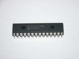
Reverse Engineering Microcontroller PIC16F73 Program
We can Reverse engineering Microcontroller PIC16F73 Program, please view the Microcontroller PIC16F73 features for your reference:
The PIC16C7X is a family of low-cost, high-performance, CMOS, fully-static, 8-bit microcontrollers with integrated analog-to-digital (A/D) converters, in the PIC16CXX mid-range family.
All PIC16/17 microcontrollers employ an advanced RISC architecture. The PIC16CXX microcontroller family has enhanced core features, eight-level deep stack, and multiple internal and external interrupt sources.
The separate instruction and data buses of the Harvard architecture allow a 14-bit wide instruction word with the separate 8-bit wide data. The two stage instruction pipeline allows all instructions to execute in a single cycle, except for program branches which require two cycles.
A total of 35 instructions (reduced instruction set) are available. Additionally, a large register set gives some of the architectural innovations used to achieve a very high performance. PIC16CXX microcontrollers typically achieve a 2:1 code compression and a 4:1 speed improvement over other 8-bit microcontrollers in their class.
The PIC16C72 has 128 bytes of RAM and 22 I/O pins. In addition several peripheral features are available including: three timer/counters, one Capture/Compare/PWM module and one serial port. The Synchronous Serial Port can be configured as either a 3-wire Serial Peripheral Interface (SPI) or the two-wire Inter-Integrated Circuit (I 2C) bus.
Also a 5-channel high-speed 8-bit A/D is provided. The 8-bit resolution is ideally suited for applications requiring low-cost analog interface, e.g. thermostat control, pressure sensing, etc.
Reverse Engineering Microcontroller PIC16F73 Program
The PIC16C73 devices have 192 bytes of RAM, while the PIC16C76 has 368 byes of RAM. Each device has 22 I/O pins. In addition, several peripheral features are available including: three timer/counters, two Capsuited for applications requiring low-cost analog interface, e.g. thermostat control, pressure sensing, etc only when Attack IC PIC12F510 Program.
The PIC16C7X family has special features to reduce external components, thus reducing cost, enhancing system reliability and reducing power consumption.
There are four oscillator options, of which the single pin RC oscillator provides a low-cost solution, the LP oscillator minimizes power consumption, XT is a standard crystal, and the HS is for High Speed crystals.
The SLEEP (power-down) feature provides a power saving mode. The user can wake up the chip from SLEEP through several external and internal interrupts and resets in order to Copy IC PIC12C509A Binary.
A highly reliable Watchdog Timer with its own on-chip RC oscillator provides protection against software lock up. A UV erasable CERDIP packaged version is ideal for code development while the cost-effective One-Time-Programmable (OTP) version is suitable for production in any volume.
The PIC16C7X family fits perfectly in applications ranging from security and remote sensors to appliance control and automotive. The EPROM technology makes customization of application programs (transmitter codes, motor speeds, receiver frequencies, etc.) extremely fast and convenient when Reverse Engineering Microcontroller PIC16F73 Program.
The small footprint packages make this microcontroller series perfect for all applications with space limitations. Low cost, low power, high performance, ease of use and I/O flexibility make the PIC16C7X very versatile even in areas where no microcontroller use has been considered (e.g. timer functions, serial communication, capture and compare, PWM functions and coprocessor applications).
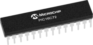
Recover MCU PIC16C72 Software
We can Recover MCU PIC16C72 Software, please see the MCU PIC16C72 features for your reference:
PIC16C7X Microcontroller Core Features:
· High-performance RISC CPU
· Only 35 single word instructions to learn
· All single cycle instructions except for program branches which are two cycle
· Operating speed: DC – 20 MHz clock input DC – 200 ns instruction cycle
· Up to 8K x 14 words of Program Memory, up to 368 x 8 bytes of Data Memory (RAM)
· Interrupt capability
· Eight level deep hardware stack
· Direct, indirect, and relative addressing modes
· Power-on Reset (POR) to facilitate the process of Recover Chip PIC16C73B Firmware
· Power-up Timer (PWRT) and Oscillator Start-up Timer (OST)
· Watchdog Timer (WDT) with its own on-chip RC oscillator for reliable operation
· Programmable code-protection
· Power saving SLEEP mode
· Selectable oscillator options
· Low-power, high-speed CMOS EPROM technology which is quite common for MCU Cracking
· Fully static design
· Wide operating voltage range: 2.5V to 6.0V
· High Sink/Source Current 25/25 mA
· Commercial, Industrial and Extended temperature ranges
· Low-power consumption:
· < 2 mA @ 5V, 4 MHz
· 15 µA typical @ 3V, 32 kHz
· < 1 µA typical standby current
PIC16C7X Peripheral Features:
· Timer0: 8-bit timer/counter with 8-bit prescaler
· Timer1: 16-bit timer/counter with prescaler, can be incremented during sleep via external crystal/clock
· Timer2: 8-bit timer/counter with 8-bit period register, prescaler and postscaler
· Capture, Compare, PWM module(s)
Recover MCU PIC16C72 Software
· Capture is 16-bit, max. resolution is 12.5 ns, Compare is 16-bit, max. resolution is 200 ns, PWM max. resolution is 10-bit
· 8-bit multichannel analog-to-digital converter
· Synchronous Serial Port (SSP) with SPI and I2C
· Universal Synchronous Asynchronous Receiver Transmitter (USART/SCI)
· Parallel Slave Port (PSP) 8-bits wide, with external RD, WR and CS controls before Recover MCU PIC16C63A Firmware
· Brown-out detection circuitry for Brown-out Reset (BOR)
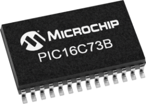
Recover Chip PIC16C73B Firmware
A highly reliable Watchdog Timer (WDT), with its own on-chip RC oscillator, provides protection against software lockup when Recover Chip PIC16C73B Firmware, and also provides one way of waking the device from SLEEP. A UV erasable CERDIP packaged version is ideal for code development, while the cost effective One-Time-Programmable (OTP) version is suitable for production in any volume.
The PIC16C73B devices fit nicely in many applications ranging from security and remote sensors to appliance control and automotive. The EPROM technology makes customization of application programs (transmitter codes, motor speeds, receiver frequencies, etc.) extremely fast and convenient.
The small footprint packages make this microcontroller series perfect for all applications with space limitations. Low cost, low power, high performance, ease of use and I/O flexibility make the PIC16C65B devices very versatile, even in areas where no microcontroller use has been considered before (e.g., timer functions, serial communication, capture and compare, PWM functions and coprocessor applications).
Users familiar with the PIC16C5X microcontroller family will realize that this is an enhanced version of the PIC16C5X architecture. Please refer to Appendix A for a detailed list of enhancements. Code written for the PIC16C5X can be easily ported to the PIC16CXX family of devices which can be used for Recover MCU 12F508 Code.
Recover Chip PIC16C73B Firmware
PICmicro® devices are supported by the complete line of Microchip Development tools. Please refer to Section 15.0 for more details about Microchip’s development tools which can also being used for Microcontroller Unlocking.
A variety of frequency ranges and packaging options are available. Depending on application and production requirements, the proper device option can be selected using the information in the PIC16C73B Product Identification System section at the end of this data sheet.
When placing orders, please use that page of the data sheet to specify the correct part number. For the PIC16C7X family, there are two device “types” as indicated in the device number.